DEMO9S08EL32 Freescale Semiconductor, DEMO9S08EL32 Datasheet - Page 345
DEMO9S08EL32
Manufacturer Part Number
DEMO9S08EL32
Description
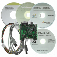
BOARD DEMO FOR 9S08 EL MCU
Manufacturer
Freescale Semiconductor
Type
MCUr
Datasheets
1.DEMO9S08EL32.pdf
(356 pages)
2.DEMO9S08EL32.pdf
(14 pages)
3.DEMO9S08EL32.pdf
(2 pages)
Specifications of DEMO9S08EL32
Contents
Evaluation Board
Processor To Be Evaluated
MC9S08EL32
Data Bus Width
8 bit
Interface Type
RS-232, USB
Operating Supply Voltage
12 V
Silicon Manufacturer
Freescale
Core Architecture
HCS08
Core Sub-architecture
HCS08
Silicon Core Number
MC9S08
Silicon Family Name
S08EL
Rohs Compliant
Yes
For Use With/related Products
MC9S08EL32
Lead Free Status / RoHS Status
Lead free / RoHS Compliant


1
2
3
A.12 AC Characteristics
This section describes ac timing characteristics for each peripheral system.
A.12.1
Freescale Semiconductor
1
2
3
4
5
Typical values assume V
and are not tested in production.
1 LSB = (V
Based on input pad leakage current. Refer to pad electricals.
Num
Characteristic
Typical values are based on characterization data at V
This is the shortest pulse that is guaranteed to be recognized as a reset pin request. Shorter pulses are not guaranteed to
override reset requests from internal sources.
When any reset is initiated, internal circuitry drives the reset pin low for about 66 cycles of t
frequency changes to the untrimmed DCO frequency (f
to 0, and there is an extra divide-by-two because BDIV is reset to 0:1. After other resets trim stays at the pre-reset value.
This is the minimum pulse width that is guaranteed to pass through the pin synchronization circuitry. Shorter pulses may or
may not be recognized. In stop mode, the synchronizer is bypassed so shorter pulses can be recognized in that case.
Timing is shown with respect to 20% V
Temp sensor
Temp sensor
1
2
3
4
5
6
voltage
slope
C
D
D
D
D
D
C
REFH
Control Timing
Bus frequency (t
Internal low power oscillator period
External reset pulse width
Reset low drive
Pin interrupt pulse width
Port rise and fall time —
Low output drive (PTxDS = 0) (load = 50 pF)
Port rise and fall time —
High output drive (PTxDS = 1) (load = 50 pF)
Asynchronous path
Synchronous path
- V
Slew rate control disabled (PTxSE = 0)
Slew rate control enabled (PTxSE = 1)
Slew rate control enabled (PTxSE = 1)
Slew rate control disabled (PTxSE = 0)
REFL
-40°C to 25°C
25°C to 125°C
25°C
)/2
DD
N
= 5.0 V, Temp = 25°C, f
MC9S08EL32 Series and MC9S08SL16 Series Data Sheet, Rev. 3
Conditions
3
cyc
= 1/f
4
2
Table A-12. ADC Characteristics (continued)
Rating
Bus
2
DD
)
and 80% V
Table A-13. Control Timing
ADCK
C
D
D
DD
= 1.0 MHz unless otherwise stated. Typical values are for reference only
DD
reset
V
levels. Temperature range –40°C to 125°C.
Symb
TEMP25
5
= 5.0V, 25°C unless otherwise stated.
5
m
= (f
dco_ut
)/4) because TRIM is reset to 0x80 and FTRIM is reset
Min
t
t
t
Symbol
—
—
—
ILIH,
Rise
Rise
t
t
t
rstdrv
f
extrst
LPO
Bus
, t
, t
t
IHIL
Fall
Fall
3.266
3.638
1.396
Typ
1.5 x t
66 x t
1
Min
800
100
100
dc
—
—
—
—
cyc
Appendix A Electrical Characteristics
cyc
cyc
Max
—
—
—
. After POR reset, the bus clock
Typ
40
75
11
35
—
—
mV/°C
Unit
1
V
1500
Max
20
—
—
—
—
—
—
—
Comment
MHz
Unit
μs
ns
ns
ns
ns
ns
347
Related parts for DEMO9S08EL32
Image
Part Number
Description
Manufacturer
Datasheet
Request
R

Part Number:
Description:
Manufacturer:
Freescale Semiconductor, Inc
Datasheet:
Part Number:
Description:
Manufacturer:
Freescale Semiconductor, Inc
Datasheet:
Part Number:
Description:
Manufacturer:
Freescale Semiconductor, Inc
Datasheet:
Part Number:
Description:
Manufacturer:
Freescale Semiconductor, Inc
Datasheet:
Part Number:
Description:
Manufacturer:
Freescale Semiconductor, Inc
Datasheet:
Part Number:
Description:
Manufacturer:
Freescale Semiconductor, Inc
Datasheet:
Part Number:
Description:
Manufacturer:
Freescale Semiconductor, Inc
Datasheet:
Part Number:
Description:
Manufacturer:
Freescale Semiconductor, Inc
Datasheet:
Part Number:
Description:
Manufacturer:
Freescale Semiconductor, Inc
Datasheet:
Part Number:
Description:
Manufacturer:
Freescale Semiconductor, Inc
Datasheet:
Part Number:
Description:
Manufacturer:
Freescale Semiconductor, Inc
Datasheet:
Part Number:
Description:
Manufacturer:
Freescale Semiconductor, Inc
Datasheet:
Part Number:
Description:
Manufacturer:
Freescale Semiconductor, Inc
Datasheet:
Part Number:
Description:
Manufacturer:
Freescale Semiconductor, Inc
Datasheet:
Part Number:
Description:
Manufacturer:
Freescale Semiconductor, Inc
Datasheet: