DEMO9S08EL32 Freescale Semiconductor, DEMO9S08EL32 Datasheet - Page 161
DEMO9S08EL32
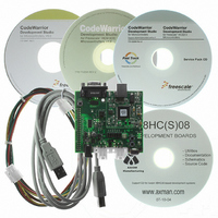
Manufacturer Part Number
DEMO9S08EL32
Description
BOARD DEMO FOR 9S08 EL MCU
Manufacturer
Freescale Semiconductor
Type
MCUr
Datasheets
1.DEMO9S08EL32.pdf
(356 pages)
2.DEMO9S08EL32.pdf
(14 pages)
3.DEMO9S08EL32.pdf
(2 pages)
Specifications of DEMO9S08EL32
Contents
Evaluation Board
Processor To Be Evaluated
MC9S08EL32
Data Bus Width
8 bit
Interface Type
RS-232, USB
Operating Supply Voltage
12 V
Silicon Manufacturer
Freescale
Core Architecture
HCS08
Core Sub-architecture
HCS08
Silicon Core Number
MC9S08
Silicon Family Name
S08EL
Rohs Compliant
Yes
For Use With/related Products
MC9S08EL32
Lead Free Status / RoHS Status
Lead free / RoHS Compliant


10.6.2
Several sources of error exist for A/D conversions. These are discussed in the following sections.
10.6.2.1
For proper conversions, the input must be sampled long enough to achieve the proper accuracy. Given the
maximum input resistance of approximately 7kΩ and input capacitance of approximately 5.5 pF, sampling
to within 1/4
8 MHz maximum ADCK frequency) provided the resistance of the external analog source (R
below 5 kΩ.
Higher source resistances or higher-accuracy sampling is possible by setting ADLSMP (to increase the
sample window to 23.5 cycles) or decreasing ADCK frequency to increase sample time.
10.6.2.2
Leakage on the I/O pins can cause conversion error if the external analog source resistance (R
If this error cannot be tolerated by the application, keep R
1/4
10.6.2.3
System noise which occurs during the sample or conversion process can affect the accuracy of the
conversion. The ADC accuracy numbers are guaranteed as specified only if the following conditions are
met:
There are some situations where external system activity causes radiated or conducted noise emissions or
excessive V
wait or stop3 or I/O activity cannot be halted, these recommended actions may reduce the effect of noise
on the accuracy:
Freescale Semiconductor
LSB
•
•
•
•
•
•
•
leakage error (N = 8 in 8-bit mode or 10 in 10-bit mode).
There is a 0.1 μF low-ESR capacitor from V
There is a 0.1 μF low-ESR capacitor from V
If inductive isolation is used from the primary supply, an additional 1 μF capacitor is placed from
V
V
Operate the MCU in wait or stop3 mode before initiating (hardware triggered conversions) or
immediately after initiating (hardware or software triggered conversions) the ADC conversion.
— For software triggered conversions, immediately follow the write to the ADCSC1 with a WAIT
— For stop3 mode operation, select ADACK as the clock source. Operation in stop3 reduces V
There is no I/O switching, input or output, on the MCU during the conversion.
Place a 0.01 μF capacitor (C
improve noise issues but will affect sample rate based on the external analog source resistance).
DDAD
SSAD
instruction or STOP instruction.
noise but increases effective conversion time due to stop recovery.
Sources of Error
DD
LSB
Sampling Error
Pin Leakage Error
Noise-Induced Errors
(and V
noise is coupled into the ADC. In these situations, or when the MCU cannot be placed in
to V
(at 10-bit resolution) can be achieved within the minimum sample window (3.5 cycles @
SSAD
REFL
MC9S08EL32 Series and MC9S08SL16 Series Data Sheet, Rev. 3
.
, if connected) is connected to V
AS
) on the selected input channel to V
REFH
DDAD
AS
to V
to V
SS
lower than V
at a quiet point in the ground plane.
REFL
SSAD
.
.
Analog-to-Digital Converter (S08ADC10V1)
DDAD
REFL
/ (2
or V
N
*I
SSAD
LEAK
(this will
) for less than
AS
AS
) is kept
) is high.
DD
161
Related parts for DEMO9S08EL32
Image
Part Number
Description
Manufacturer
Datasheet
Request
R

Part Number:
Description:
Manufacturer:
Freescale Semiconductor, Inc
Datasheet:
Part Number:
Description:
Manufacturer:
Freescale Semiconductor, Inc
Datasheet:
Part Number:
Description:
Manufacturer:
Freescale Semiconductor, Inc
Datasheet:
Part Number:
Description:
Manufacturer:
Freescale Semiconductor, Inc
Datasheet:
Part Number:
Description:
Manufacturer:
Freescale Semiconductor, Inc
Datasheet:
Part Number:
Description:
Manufacturer:
Freescale Semiconductor, Inc
Datasheet:
Part Number:
Description:
Manufacturer:
Freescale Semiconductor, Inc
Datasheet:
Part Number:
Description:
Manufacturer:
Freescale Semiconductor, Inc
Datasheet:
Part Number:
Description:
Manufacturer:
Freescale Semiconductor, Inc
Datasheet:
Part Number:
Description:
Manufacturer:
Freescale Semiconductor, Inc
Datasheet:
Part Number:
Description:
Manufacturer:
Freescale Semiconductor, Inc
Datasheet:
Part Number:
Description:
Manufacturer:
Freescale Semiconductor, Inc
Datasheet:
Part Number:
Description:
Manufacturer:
Freescale Semiconductor, Inc
Datasheet:
Part Number:
Description:
Manufacturer:
Freescale Semiconductor, Inc
Datasheet:
Part Number:
Description:
Manufacturer:
Freescale Semiconductor, Inc
Datasheet: