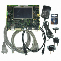
AT91SAM9G45-EKES Atmel, AT91SAM9G45-EKES Datasheet - Page 1110

AT91SAM9G45-EKES
Manufacturer Part Number
AT91SAM9G45-EKES
Description
KIT EVAL FOR AT91SAM9G45
Manufacturer
Atmel
Series
AT91SAM Smart ARMr
Type
MCUr
Datasheets
1.AT91SAM9G45-EKES.pdf
(56 pages)
2.AT91SAM9G45-EKES.pdf
(1218 pages)
3.AT91SAM9G45-EKES.pdf
(66 pages)
Specifications of AT91SAM9G45-EKES
Contents
Board
Processor To Be Evaluated
SAM9G45
Data Bus Width
32 bit
Interface Type
I2C, SPI, UART
Maximum Operating Temperature
+ 50 C
Minimum Operating Temperature
- 10 C
Operating Supply Voltage
1.8 V to 3.3 V
For Use With/related Products
AT91SAM9G45
Lead Free Status / RoHS Status
Lead free / RoHS Compliant
Other names
Q4626953
- Current page: 1110 of 1218
- Download datasheet (19Mb)
45.6.2.9
1110
AT91SAM9G45
Equation 1
There is a limitation in the minimum values of VHDLY, HPW and HBP parameters imposed by
the initial latency of the datapath. The total delay in LCDC clock cycles must be higher than or
equal to the latency column in
formula:
where:
The LCDVSYNC is asserted once per frame. This signal is asserted to cause the LCD's line
pointer to start over at the top of the display. The timing of this signal depends on the type of
LCD: STN or TFT LCD.
In STN mode, the high phase corresponds to the complete first line of the frame. In STN mode,
this signal is synchronized with the first active LCDDOTCK rising edge in a line.
In TFT mode, the high phase of this signal starts at the beginning of the first line. The following
timing parameters can be selected:
There are two other parameters to configure in this module, the HOZVAL and the LINEVAL
fields of the LCDFRMCFG:
• Vertical to Horizontal Delay (VHDLY): The delay between the falling edge of LCDVSYNC and
• Horizontal Pulse Width (HPW): The LCDHSYNC pulse width is configurable in HPW field of
• Horizontal Back Porch (HBP): The delay between the LCDHSYNC falling edge and the first
• Horizontal Front Porch (HFP): The delay between end of valid data and the generation of the
• VHDLY, HPW, HBP are the value of the fields of LCDTIM1 and LCDTIM2 registers
• PCLK_PERIOD is the period of LCDDOTCK signal measured in LCDC Clock cycles
• DPATH_LATENCY is the datapath latency of the configuration, given in
• Vertical Pulse Width (VPW): LCDVSYNC pulse width is configurable in VPW field of the
• Vertical Back Porch: Number of inactive lines at the beginning of the frame is configurable in
• Vertical Front Porch: Number of inactive lines at the end of the frame is configurable in VFP
• HOZVAL configures the number of active LCDDOTCK cycles in each line. The number of
the generation of LCDHSYNC is configurable in the VHDLY field of the LCDTIM1 register.
The delay is equal to (VHDLY+1) LCDDOTCK cycles.
LCDTIM2 register. The width is equal to (HPW + 1) LCDDOTCK cycles.
LCDDOTCK rising edge with valid data at the LCD Interface is configurable in the HBP field
of the LCDTIM2 register. The delay is equal to (HBP+1) LCDDOTCK cycles.
next LCDHSYNC is configurable in the HFP field of the LCDTIM2 register. The delay is equal
to (HFP+VHDLY+2) LCDDOTCK cycles.
1102
LCDTIM1 register. The pulse width is equal to (VPW+1) lines.
VBP field of LCDTIM1 register. The number of inactive lines is equal to VBP. This field should
be programmed with 0 in STN Mode.
field of LCDTIM2 register. The number of inactive lines is equal to VFP. This field should be
programmed with 0 in STN mode.
active cycles in each line is equal to (HOZVAL+1) cycles. The minimum value of this
parameter is 1.
VHDLY
+
HPW
Table 45-4 on page
+
HBP
+
3
PCLK_PERIOD
1102. This limitation is given by the following
DPATH_LATENCY
Table 45-4 on page
6438F–ATARM–21-Jun-10
Related parts for AT91SAM9G45-EKES
Image
Part Number
Description
Manufacturer
Datasheet
Request
R

Part Number:
Description:
MCU ARM9 64K SRAM 144-LFBGA
Manufacturer:
Atmel
Datasheet:

Part Number:
Description:
IC ARM7 MCU FLASH 256K 100LQFP
Manufacturer:
Atmel
Datasheet:

Part Number:
Description:
IC ARM9 MPU 217-LFBGA
Manufacturer:
Atmel
Datasheet:

Part Number:
Description:
MCU ARM9 ULTRA LOW PWR 217-LFBGA
Manufacturer:
Atmel
Datasheet:

Part Number:
Description:
MCU ARM9 324-TFBGA
Manufacturer:
Atmel
Datasheet:

Part Number:
Description:
IC MCU ARM9 SAMPLING 217CBGA
Manufacturer:
Atmel
Datasheet:

Part Number:
Description:
IC ARM9 MCU 217-LFBGA
Manufacturer:
Atmel
Datasheet:

Part Number:
Description:
IC ARM9 MCU 208-PQFP
Manufacturer:
Atmel
Datasheet:

Part Number:
Description:
MCU ARM 512K HS FLASH 100-LQFP
Manufacturer:
Atmel
Datasheet:

Part Number:
Description:
MCU ARM 512K HS FLASH 100-TFBGA
Manufacturer:
Atmel
Datasheet:

Part Number:
Description:
IC ARM9 MCU 200 MHZ 324-TFBGA
Manufacturer:
Atmel
Datasheet:

Part Number:
Description:
IC ARM MCU 16BIT 128K 256BGA
Manufacturer:
Atmel
Datasheet:

Part Number:
Description:
IC ARM7 MCU 32BIT 128K 64LQFP
Manufacturer:
Atmel
Datasheet:

Part Number:
Description:
IC ARM7 MCU FLASH 256K 128-LQFP
Manufacturer:
Atmel
Datasheet:

Part Number:
Description:
IC ARM7 MCU FLASH 512K 128-LQFP
Manufacturer:
Atmel
Datasheet:


