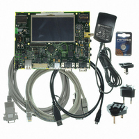
AT91SAM9G45-EKES Atmel, AT91SAM9G45-EKES Datasheet - Page 305

AT91SAM9G45-EKES
Manufacturer Part Number
AT91SAM9G45-EKES
Description
KIT EVAL FOR AT91SAM9G45
Manufacturer
Atmel
Series
AT91SAM Smart ARMr
Type
MCUr
Datasheets
1.AT91SAM9G45-EKES.pdf
(56 pages)
2.AT91SAM9G45-EKES.pdf
(1218 pages)
3.AT91SAM9G45-EKES.pdf
(66 pages)
Specifications of AT91SAM9G45-EKES
Contents
Board
Processor To Be Evaluated
SAM9G45
Data Bus Width
32 bit
Interface Type
I2C, SPI, UART
Maximum Operating Temperature
+ 50 C
Minimum Operating Temperature
- 10 C
Operating Supply Voltage
1.8 V to 3.3 V
For Use With/related Products
AT91SAM9G45
Lead Free Status / RoHS Status
Lead free / RoHS Compliant
Other names
Q4626953
- Current page: 305 of 1218
- Download datasheet (19Mb)
6438F–ATARM–21-Jun-10
3. Setting Bias and High Speed PLL (UPLL) for UTMI
4. Selection of Master Clock and Processor Clock
The DIVA field is used to control divider itself. A value between 0 and 255 can be pro-
grammed. Divider output is divider input divided by DIVA parameter. By default DIVA
parameter is set to 0 which means that divider is turned off.
The OUTA field is used to select the PLLA output frequency range.
The MULA field is the PLLA multiplier factor. This parameter can be programmed between 0
and 254. If MULA is set to 0, PLLA will be turned off, otherwise the PLLA output frequency is
PLLA input frequency multiplied by (MULA + 1).
The PLLACOUNT field specifies the number of slow clock cycles before LOCKA bit is set in
the PMC_SR register after CKGR_PLLAR register has been written.
Once the PMC_PLLAR register has been written, the user must wait for the LOCKA bit to be
set in the PMC_SR register. This can be done either by polling the status register or by wait-
ing the interrupt line to be raised if the associated interrupt to LOCKA has been enabled in
the PMC_IER register. All parameters in CKGR_PLLAR can be programmed in a single write
operation. If at some stage one of the following parameters, MULA, DIVA is modified,
LOCKA bit will go low to indicate that PLLA is not ready yet. When PLLA is locked, LOCKA
will be set again. The user is constrained to wait for LOCKA bit to be set before using the
PLLA output clock.
Code Example:
If PLLA and divider are enabled, the PLLA input clock is the main clock. PLLA output clock is
PLLA input clock multiplied by 5. Once CKGR_PLLAR has been written, LOCKA bit will be
set after eight slow clock cycles.
The UTMI PLL is enabled by setting the UPLLEN field in the CKGR_UCKR register. The
UTMI Bias must is enabled by setting the BIASEN field in the CKGR_UCKR register in the
same time. In some cases it may be advantageous to define a start-up time. This can be
achieved by writing a value in the PLLCOUNT field in the CKGR_UCKR register.
Once this register has been correctly configured, the user must wait for LOCKU field in the
PMC_SR register to be set. This can be done either by polling the status register or by wait-
ing the interrupt line to be raised if the associated interrupt to LOCKU has been enabled in
the PMC_IER register.
The Master Clock and the Processor Clock are configurable via the PMC_MCKR register.
The CSS field is used to select the clock source of the Master Clock and Processor Clock
dividers. By default, the selected clock source is slow clock.
The PRES field is used to control the Master/Processor Clock prescaler. The user can
choose between different values (1, 2, 4, 8, 16, 32, 64). Prescaler output is the selected clock
source divided by PRES parameter. By default, PRES parameter is set to 1 which means
that the input clock of the Master Clock and Processor Clock dividers is equal to slow clock.
write_register(CKGR_PLLAR,0x00040805)
AT91SAM9G45
305
Related parts for AT91SAM9G45-EKES
Image
Part Number
Description
Manufacturer
Datasheet
Request
R

Part Number:
Description:
MCU ARM9 64K SRAM 144-LFBGA
Manufacturer:
Atmel
Datasheet:

Part Number:
Description:
IC ARM7 MCU FLASH 256K 100LQFP
Manufacturer:
Atmel
Datasheet:

Part Number:
Description:
IC ARM9 MPU 217-LFBGA
Manufacturer:
Atmel
Datasheet:

Part Number:
Description:
MCU ARM9 ULTRA LOW PWR 217-LFBGA
Manufacturer:
Atmel
Datasheet:

Part Number:
Description:
MCU ARM9 324-TFBGA
Manufacturer:
Atmel
Datasheet:

Part Number:
Description:
IC MCU ARM9 SAMPLING 217CBGA
Manufacturer:
Atmel
Datasheet:

Part Number:
Description:
IC ARM9 MCU 217-LFBGA
Manufacturer:
Atmel
Datasheet:

Part Number:
Description:
IC ARM9 MCU 208-PQFP
Manufacturer:
Atmel
Datasheet:

Part Number:
Description:
MCU ARM 512K HS FLASH 100-LQFP
Manufacturer:
Atmel
Datasheet:

Part Number:
Description:
MCU ARM 512K HS FLASH 100-TFBGA
Manufacturer:
Atmel
Datasheet:

Part Number:
Description:
IC ARM9 MCU 200 MHZ 324-TFBGA
Manufacturer:
Atmel
Datasheet:

Part Number:
Description:
IC ARM MCU 16BIT 128K 256BGA
Manufacturer:
Atmel
Datasheet:

Part Number:
Description:
IC ARM7 MCU 32BIT 128K 64LQFP
Manufacturer:
Atmel
Datasheet:

Part Number:
Description:
IC ARM7 MCU FLASH 256K 128-LQFP
Manufacturer:
Atmel
Datasheet:

Part Number:
Description:
IC ARM7 MCU FLASH 512K 128-LQFP
Manufacturer:
Atmel
Datasheet:


