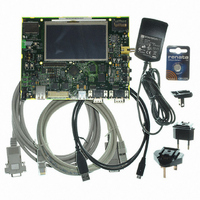
AT91SAM9G45-EKES Atmel, AT91SAM9G45-EKES Datasheet - Page 304

AT91SAM9G45-EKES
Manufacturer Part Number
AT91SAM9G45-EKES
Description
KIT EVAL FOR AT91SAM9G45
Manufacturer
Atmel
Series
AT91SAM Smart ARMr
Type
MCUr
Datasheets
1.AT91SAM9G45-EKES.pdf
(56 pages)
2.AT91SAM9G45-EKES.pdf
(1218 pages)
3.AT91SAM9G45-EKES.pdf
(66 pages)
Specifications of AT91SAM9G45-EKES
Contents
Board
Processor To Be Evaluated
SAM9G45
Data Bus Width
32 bit
Interface Type
I2C, SPI, UART
Maximum Operating Temperature
+ 50 C
Minimum Operating Temperature
- 10 C
Operating Supply Voltage
1.8 V to 3.3 V
For Use With/related Products
AT91SAM9G45
Lead Free Status / RoHS Status
Lead free / RoHS Compliant
Other names
Q4626953
- Current page: 304 of 1218
- Download datasheet (19Mb)
25.7
25.8
25.9
304
Peripheral Clock Controller
Programmable Clock Output Controller
Programming Sequence
AT91SAM9G45
The Power Management Controller controls the clocks of each embedded peripheral by the way
of the Peripheral Clock Controller. The user can individually enable and disable the Master
Clock on the peripherals by writing into the Peripheral Clock Enable (PMC_PCER) and Periph-
eral Clock Disable (PMC_PCDR) registers. The status of the peripheral clock activity can be
read in the Peripheral Clock Status Register (PMC_PCSR).
When a peripheral clock is disabled, the clock is immediately stopped. The peripheral clocks are
automatically disabled after a reset.
In order to stop a peripheral, it is recommended that the system software wait until the peripheral
has executed its last programmed operation before disabling the clock. This is to avoid data cor-
ruption or erroneous behavior of the system.
The bit number within the Peripheral Clock Control registers (PMC_PCER, PMC_PCDR, and
PMC_PCSR) is the Peripheral Identifier defined at the product level. Generally, the bit number
corresponds to the interrupt source number assigned to the peripheral.
The PMC controls PMC_PROG_CLK_NB signals to be output on external pins PCKx. Each sig-
nal can be independently programmed via the PMC_PCKx registers.
PCKx can be independently selected between the Slow clock, the Master Clock, the
PLLACK/PLLADIV2, the UTMI PLL output and the main clock by writing the CSS and CSSMCK
fields in PMC_PCKx. Each output signal can also be divided by a power of 2 between 1 and 64
by writing the PRES (Prescaler) field in PMC_PCKx.
Each output signal can be enabled and disabled by writing 1 in the corresponding bit, PCKx of
PMC_SCER and PMC_SCDR, respectively. Status of the active programmable output clocks
are given in the PCKx bits of PMC_SCSR (System Clock Status Register).
Moreover, like the PCK, a status bit in PMC_SR indicates that the Programmable Clock is actu-
ally what has been programmed in the Programmable Clock registers.
As the Programmable Clock Controller does not manage with glitch prevention when switching
clocks, it is strongly recommended to disable the Programmable Clock before any configuration
change and to re-enable it after the change is actually performed.
1. Enabling the 12MHz Main Oscillator:
2. Setting PLLA and divider:
The main oscillator is enabled by setting the MOSCEN field in the CKGR_MOR register. In
some cases it may be advantageous to define a start-up time. This can be achieved by writ-
ing a value in the OSCOUNT field in the CKGR_MOR register.
Once this register has been correctly configured, the user must wait for MOSCS field in the
PMC_SR register to be set. This can be done either by polling the status register or by wait-
ing the interrupt line to be raised if the associated interrupt to MOSCS has been enabled in
the PMC_IER register.
All parameters needed to configure PLLA and the divider are located in the CKGR_PLLAR
register.
6438F–ATARM–21-Jun-10
Related parts for AT91SAM9G45-EKES
Image
Part Number
Description
Manufacturer
Datasheet
Request
R

Part Number:
Description:
MCU ARM9 64K SRAM 144-LFBGA
Manufacturer:
Atmel
Datasheet:

Part Number:
Description:
IC ARM7 MCU FLASH 256K 100LQFP
Manufacturer:
Atmel
Datasheet:

Part Number:
Description:
IC ARM9 MPU 217-LFBGA
Manufacturer:
Atmel
Datasheet:

Part Number:
Description:
MCU ARM9 ULTRA LOW PWR 217-LFBGA
Manufacturer:
Atmel
Datasheet:

Part Number:
Description:
MCU ARM9 324-TFBGA
Manufacturer:
Atmel
Datasheet:

Part Number:
Description:
IC MCU ARM9 SAMPLING 217CBGA
Manufacturer:
Atmel
Datasheet:

Part Number:
Description:
IC ARM9 MCU 217-LFBGA
Manufacturer:
Atmel
Datasheet:

Part Number:
Description:
IC ARM9 MCU 208-PQFP
Manufacturer:
Atmel
Datasheet:

Part Number:
Description:
MCU ARM 512K HS FLASH 100-LQFP
Manufacturer:
Atmel
Datasheet:

Part Number:
Description:
MCU ARM 512K HS FLASH 100-TFBGA
Manufacturer:
Atmel
Datasheet:

Part Number:
Description:
IC ARM9 MCU 200 MHZ 324-TFBGA
Manufacturer:
Atmel
Datasheet:

Part Number:
Description:
IC ARM MCU 16BIT 128K 256BGA
Manufacturer:
Atmel
Datasheet:

Part Number:
Description:
IC ARM7 MCU 32BIT 128K 64LQFP
Manufacturer:
Atmel
Datasheet:

Part Number:
Description:
IC ARM7 MCU FLASH 256K 128-LQFP
Manufacturer:
Atmel
Datasheet:

Part Number:
Description:
IC ARM7 MCU FLASH 512K 128-LQFP
Manufacturer:
Atmel
Datasheet:


