AT91SAM9G45-EKES Atmel, AT91SAM9G45-EKES Datasheet - Page 357

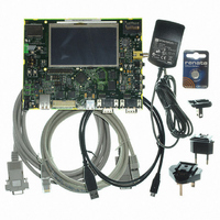
AT91SAM9G45-EKES
Manufacturer Part Number
AT91SAM9G45-EKES
Description
KIT EVAL FOR AT91SAM9G45
Manufacturer
Atmel
Series
AT91SAM Smart ARMr
Type
MCUr
Datasheets
1.AT91SAM9G45-EKES.pdf
(56 pages)
2.AT91SAM9G45-EKES.pdf
(1218 pages)
3.AT91SAM9G45-EKES.pdf
(66 pages)
Specifications of AT91SAM9G45-EKES
Contents
Board
Processor To Be Evaluated
SAM9G45
Data Bus Width
32 bit
Interface Type
I2C, SPI, UART
Maximum Operating Temperature
+ 50 C
Minimum Operating Temperature
- 10 C
Operating Supply Voltage
1.8 V to 3.3 V
For Use With/related Products
AT91SAM9G45
Lead Free Status / RoHS Status
Lead free / RoHS Compliant
Other names
Q4626953
- Current page: 357 of 1218
- Download datasheet (19Mb)
27.4
27.4.1
27.4.2
27.4.3
27.5
27.5.1
6438F–ATARM–21-Jun-10
Product Dependencies
UART Operations
I/O Lines
Power Management
Interrupt Source
Baud Rate Generator
Depending on product integration, the Debug Unit pins may be multiplexed with PIO lines. In this
case, the programmer must first configure the corresponding PIO Controller to enable I/O lines
operations of the Debug Unit.
Table 27-2.
Depending on product integration, the Debug Unit clock may be controllable through the Power
Management Controller. In this case, the programmer must first configure the PMC to enable the
Debug Unit clock. Usually, the peripheral identifier used for this purpose is 1.
Depending on product integration, the Debug Unit interrupt line is connected to one of the inter-
rupt sources of the Advanced Interrupt Controller. Interrupt handling requires programming of
the AIC before configuring the Debug Unit. Usually, the Debug Unit interrupt line connects to the
interrupt source 1 of the AIC, which may be shared with the real-time clock, the system timer
interrupt lines and other system peripheral interrupts, as shown in
requires the programmer to determine the source of the interrupt when the source 1 is triggered.
The Debug Unit operates as a UART, (asynchronous mode only) and supports only 8-bit charac-
ter handling (with parity). It has no clock pin.
The Debug Unit's UART is made up of a receiver and a transmitter that operate independently,
and a common baud rate generator. Receiver timeout and transmitter time guard are not imple-
mented. However, all the implemented features are compatible with those of a standard USART.
The baud rate generator provides the bit period clock named baud rate clock to both the receiver
and the transmitter.
The baud rate clock is the master clock divided by 16 times the value (CD) written in
DBGU_BRGR (Baud Rate Generator Register). If DBGU_BRGR is set to 0, the baud rate clock
is disabled and the Debug Unit's UART remains inactive. The maximum allowable baud rate is
Master Clock divided by 16. The minimum allowable baud rate is Master Clock divided by (16 x
65536).
Instance
DBGU
DBGU
I/O Lines
Baud Rate
Signal
DRXD
DTXD
=
-------------------- -
16
MCK
CD
I/O Line
PB12
PB13
AT91SAM9G45
Figure
27-1. This sharing
Peripheral
A
A
357
Related parts for AT91SAM9G45-EKES
Image
Part Number
Description
Manufacturer
Datasheet
Request
R

Part Number:
Description:
MCU ARM9 64K SRAM 144-LFBGA
Manufacturer:
Atmel
Datasheet:

Part Number:
Description:
IC ARM7 MCU FLASH 256K 100LQFP
Manufacturer:
Atmel
Datasheet:

Part Number:
Description:
IC ARM9 MPU 217-LFBGA
Manufacturer:
Atmel
Datasheet:

Part Number:
Description:
MCU ARM9 ULTRA LOW PWR 217-LFBGA
Manufacturer:
Atmel
Datasheet:

Part Number:
Description:
MCU ARM9 324-TFBGA
Manufacturer:
Atmel
Datasheet:

Part Number:
Description:
IC MCU ARM9 SAMPLING 217CBGA
Manufacturer:
Atmel
Datasheet:

Part Number:
Description:
IC ARM9 MCU 217-LFBGA
Manufacturer:
Atmel
Datasheet:

Part Number:
Description:
IC ARM9 MCU 208-PQFP
Manufacturer:
Atmel
Datasheet:

Part Number:
Description:
MCU ARM 512K HS FLASH 100-LQFP
Manufacturer:
Atmel
Datasheet:

Part Number:
Description:
MCU ARM 512K HS FLASH 100-TFBGA
Manufacturer:
Atmel
Datasheet:

Part Number:
Description:
IC ARM9 MCU 200 MHZ 324-TFBGA
Manufacturer:
Atmel
Datasheet:

Part Number:
Description:
IC ARM MCU 16BIT 128K 256BGA
Manufacturer:
Atmel
Datasheet:

Part Number:
Description:
IC ARM7 MCU 32BIT 128K 64LQFP
Manufacturer:
Atmel
Datasheet:

Part Number:
Description:
IC ARM7 MCU FLASH 256K 128-LQFP
Manufacturer:
Atmel
Datasheet:

Part Number:
Description:
IC ARM7 MCU FLASH 512K 128-LQFP
Manufacturer:
Atmel
Datasheet:


