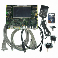
AT91SAM9G45-EKES Atmel, AT91SAM9G45-EKES Datasheet - Page 1121

AT91SAM9G45-EKES
Manufacturer Part Number
AT91SAM9G45-EKES
Description
KIT EVAL FOR AT91SAM9G45
Manufacturer
Atmel
Series
AT91SAM Smart ARMr
Type
MCUr
Datasheets
1.AT91SAM9G45-EKES.pdf
(56 pages)
2.AT91SAM9G45-EKES.pdf
(1218 pages)
3.AT91SAM9G45-EKES.pdf
(66 pages)
Specifications of AT91SAM9G45-EKES
Contents
Board
Processor To Be Evaluated
SAM9G45
Data Bus Width
32 bit
Interface Type
I2C, SPI, UART
Maximum Operating Temperature
+ 50 C
Minimum Operating Temperature
- 10 C
Operating Supply Voltage
1.8 V to 3.3 V
For Use With/related Products
AT91SAM9G45
Lead Free Status / RoHS Status
Lead free / RoHS Compliant
Other names
Q4626953
- Current page: 1121 of 1218
- Download datasheet (19Mb)
6438F–ATARM–21-Jun-10
• Configure the DMA Controller. The user should configure the base address of the display
• Finally, enable the LCD Controller Core by writing a “1” in the LCD_PWR field of the
buffer memory, the size of the AHB transaction and the size of the display image in memory.
When the DMA is configured the user should enable the DMA. To do so the user should
configure the following registers:
PWRCON register and do any other action that may be required to turn the LCD module on.
– LCDCON2 register: Program its fields following their descriptions in the LCD
– LCDTIM1 and LCDTIM2 registers: Program their fields according to the datasheet of
– LCDFRMCFG register: program the dimensions of the LCD module used.
– LCDFIFO register: To program it, use the formula in section
– LCDMVAL register: Its configuration depends on the LCD Module used and should
– DP1_2 to DP6_7 registers: they are only used for STN displays. They contain the
– PWRCON Register: this register controls the power-up sequence of the LCD, so
– CONTRAST_CTR and CONTRAST_VAL: use this registers to adjust the contrast of
– DMABADDR1 and DMABADDR2 registers: In single scan mode only DMABADDR1
– DMAFRMCFG register: Program the FRMSIZE field. Note that in dual scan mode
– DMACON register: Once both the LCD Controller Core and the DMA Controller have
– DMA2DCFG register: Required only in 2D memory addressing mode (see
Controller User Interface section below and considering the type of LCD module
used and the desired working mode. Consider that not all combinations are possible.
the LCD module used and with the help of the Timegen section in page 10. Note that
some fields are not applicable to STN modules and must be programmed with 0
values. Note also that there is a limitation on the minimum value of VHDLY, HPW,
HBP that depends on the configuration of the LCDC.
be tuned to improve the image quality in the display
dithering patterns used to generate gray shades or colors in these modules. They
are loaded with recommended patterns at reset, so it is not necessary to write
anything on them. They can be used to improve the image quality in the display by
tuning the patterns in each application.
take care to use it properly. Do not enable the LCD (writing a 1 in LCD_PWR field)
until the previous steps and the configuration of the DMA have been finished.
the display, when the LCDCC line is used.
register must be configured with the base address of the display buffer in memory. In
dual scan mode DMABADDR1 should be configured with the base address of the
Upper Panel display buffer and DMABADDR2 should be configured with the base
address of the Lower Panel display buffer.
the vertical size to use in the calculation is that of each panel. Respect to the
BRSTLN field, a recommended value is a 4-word burst.
been configured, enable the DMA Controller by writing a “1” to the DMAEN field of
this register. If using a dual scan module or the 2D addressing feature, do not forget
to write the DMAUPDT bit after every change to the set of DMA configuration values.
Memory Addressing” on page
1122).
(See “Timegen” on page
AT91SAM9G45
“FIFO” on page 1102
“2D
1108.)
1121
Related parts for AT91SAM9G45-EKES
Image
Part Number
Description
Manufacturer
Datasheet
Request
R

Part Number:
Description:
MCU ARM9 64K SRAM 144-LFBGA
Manufacturer:
Atmel
Datasheet:

Part Number:
Description:
IC ARM7 MCU FLASH 256K 100LQFP
Manufacturer:
Atmel
Datasheet:

Part Number:
Description:
IC ARM9 MPU 217-LFBGA
Manufacturer:
Atmel
Datasheet:

Part Number:
Description:
MCU ARM9 ULTRA LOW PWR 217-LFBGA
Manufacturer:
Atmel
Datasheet:

Part Number:
Description:
MCU ARM9 324-TFBGA
Manufacturer:
Atmel
Datasheet:

Part Number:
Description:
IC MCU ARM9 SAMPLING 217CBGA
Manufacturer:
Atmel
Datasheet:

Part Number:
Description:
IC ARM9 MCU 217-LFBGA
Manufacturer:
Atmel
Datasheet:

Part Number:
Description:
IC ARM9 MCU 208-PQFP
Manufacturer:
Atmel
Datasheet:

Part Number:
Description:
MCU ARM 512K HS FLASH 100-LQFP
Manufacturer:
Atmel
Datasheet:

Part Number:
Description:
MCU ARM 512K HS FLASH 100-TFBGA
Manufacturer:
Atmel
Datasheet:

Part Number:
Description:
IC ARM9 MCU 200 MHZ 324-TFBGA
Manufacturer:
Atmel
Datasheet:

Part Number:
Description:
IC ARM MCU 16BIT 128K 256BGA
Manufacturer:
Atmel
Datasheet:

Part Number:
Description:
IC ARM7 MCU 32BIT 128K 64LQFP
Manufacturer:
Atmel
Datasheet:

Part Number:
Description:
IC ARM7 MCU FLASH 256K 128-LQFP
Manufacturer:
Atmel
Datasheet:

Part Number:
Description:
IC ARM7 MCU FLASH 512K 128-LQFP
Manufacturer:
Atmel
Datasheet:


