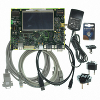
AT91SAM9G45-EKES Atmel, AT91SAM9G45-EKES Datasheet - Page 1204

AT91SAM9G45-EKES
Manufacturer Part Number
AT91SAM9G45-EKES
Description
KIT EVAL FOR AT91SAM9G45
Manufacturer
Atmel
Series
AT91SAM Smart ARMr
Type
MCUr
Datasheets
1.AT91SAM9G45-EKES.pdf
(56 pages)
2.AT91SAM9G45-EKES.pdf
(1218 pages)
3.AT91SAM9G45-EKES.pdf
(66 pages)
Specifications of AT91SAM9G45-EKES
Contents
Board
Processor To Be Evaluated
SAM9G45
Data Bus Width
32 bit
Interface Type
I2C, SPI, UART
Maximum Operating Temperature
+ 50 C
Minimum Operating Temperature
- 10 C
Operating Supply Voltage
1.8 V to 3.3 V
For Use With/related Products
AT91SAM9G45
Lead Free Status / RoHS Status
Lead free / RoHS Compliant
Other names
Q4626953
- Current page: 1204 of 1218
- Download datasheet (19Mb)
1204
Doc. Rev
6438D
Doc. Rev
6438C
Doc. Rev
6438B
AT91SAM9G45
Comments
LCD Controller (LCDC):
Section 45.12.12 “LCD Timing Configuration Register
written to 1’ added to VHDLY definition.
Parallel Input/Output Controller (PIO):
- DELAY Registers were addded in a
description added in a
-
Register”and
In
Clear Output Data”
All ‘slewrate’ changed into ‘drive’.
All ‘IO’ changed into ‘I/O’.
All
Any extra ‘Controller’ or ‘Controller PIO’ removed.
Static Memory Controller (SMC):
Table 21-5 removed from
21-8
USB Host Port:
Section 37. “USB High Speed Host Port (UHPHS)”
Comments
Introduction:
Section 3. “Signal Description”
concerning NRST configuration.
Section 4. “Package and
Boot Program:
Section 11.5.2.1 “Supported External Crystal/External
RSTC:
Section 12.5 “Reset Controller (RSTC) User Interface” Table 12-1
0x0000 0001.
Comments
DDRSDRC:
Section 22.7.3 “DDRSDRC Configuration
Section 22.7.9 “DDRSDRC DLL Register”
removed from register.
“Write Protected Registers”
Section 30.6.11 “PIO Clear Output Data
Section 30.6 “Parallel Input/Output Controller (PIO) User Interface”
instead.
Section 30.6.32 “PIO Write Protect Status
Section 30.6.30 “PIO I/O Delay
Pinout”,
Section 21.8.6 “Reset Values of Timing
description added, together with
,
Table
Table 4-1
Section 30.4.12 “Programmable I/O Delays”
3-1, in
Register”, bit named ENRDM removed from register.
bits named, SDCOVF, SDCUDF, SDERF, SDVAL, SDCVAL
Register”, “P0-P31: Set Output Data” changed into “P0-P31:
updated.
“Reset/Test”
, HS (High Speed) was added to the title.
1”, ‘-’ replaced by ‘1’ for bit 31, and ‘Bit 31 must be
Clocks”, ...”supports 12 MHz”...
Register”.
Register”.
description, NRST pin updated with note
Section 30.6.31 “PIO Write Protect Mode
Parameters”. Cross-referenced
Mode register backup reset value is
headers now start with ‘PIO’ only.
and associated register
Table
6438F–ATARM–21-Jun-10
Change
Request
Ref.
6685
6715
6742
6644
Change
Request
Ref.
6600
6639
6598
6639
Change
Request
Ref.
6606
Related parts for AT91SAM9G45-EKES
Image
Part Number
Description
Manufacturer
Datasheet
Request
R

Part Number:
Description:
MCU ARM9 64K SRAM 144-LFBGA
Manufacturer:
Atmel
Datasheet:

Part Number:
Description:
IC ARM7 MCU FLASH 256K 100LQFP
Manufacturer:
Atmel
Datasheet:

Part Number:
Description:
IC ARM9 MPU 217-LFBGA
Manufacturer:
Atmel
Datasheet:

Part Number:
Description:
MCU ARM9 ULTRA LOW PWR 217-LFBGA
Manufacturer:
Atmel
Datasheet:

Part Number:
Description:
MCU ARM9 324-TFBGA
Manufacturer:
Atmel
Datasheet:

Part Number:
Description:
IC MCU ARM9 SAMPLING 217CBGA
Manufacturer:
Atmel
Datasheet:

Part Number:
Description:
IC ARM9 MCU 217-LFBGA
Manufacturer:
Atmel
Datasheet:

Part Number:
Description:
IC ARM9 MCU 208-PQFP
Manufacturer:
Atmel
Datasheet:

Part Number:
Description:
MCU ARM 512K HS FLASH 100-LQFP
Manufacturer:
Atmel
Datasheet:

Part Number:
Description:
MCU ARM 512K HS FLASH 100-TFBGA
Manufacturer:
Atmel
Datasheet:

Part Number:
Description:
IC ARM9 MCU 200 MHZ 324-TFBGA
Manufacturer:
Atmel
Datasheet:

Part Number:
Description:
IC ARM MCU 16BIT 128K 256BGA
Manufacturer:
Atmel
Datasheet:

Part Number:
Description:
IC ARM7 MCU 32BIT 128K 64LQFP
Manufacturer:
Atmel
Datasheet:

Part Number:
Description:
IC ARM7 MCU FLASH 256K 128-LQFP
Manufacturer:
Atmel
Datasheet:

Part Number:
Description:
IC ARM7 MCU FLASH 512K 128-LQFP
Manufacturer:
Atmel
Datasheet:


