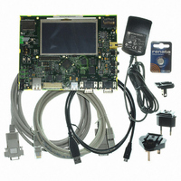
AT91SAM9G45-EKES Atmel, AT91SAM9G45-EKES Datasheet - Page 438

AT91SAM9G45-EKES
Manufacturer Part Number
AT91SAM9G45-EKES
Description
KIT EVAL FOR AT91SAM9G45
Manufacturer
Atmel
Series
AT91SAM Smart ARMr
Type
MCUr
Datasheets
1.AT91SAM9G45-EKES.pdf
(56 pages)
2.AT91SAM9G45-EKES.pdf
(1218 pages)
3.AT91SAM9G45-EKES.pdf
(66 pages)
Specifications of AT91SAM9G45-EKES
Contents
Board
Processor To Be Evaluated
SAM9G45
Data Bus Width
32 bit
Interface Type
I2C, SPI, UART
Maximum Operating Temperature
+ 50 C
Minimum Operating Temperature
- 10 C
Operating Supply Voltage
1.8 V to 3.3 V
For Use With/related Products
AT91SAM9G45
Lead Free Status / RoHS Status
Lead free / RoHS Compliant
Other names
Q4626953
- Current page: 438 of 1218
- Download datasheet (19Mb)
Figure 29-13. Slave Mode Functional Bloc Diagram
438
AT91SAM9G45
SPCK
MOSI
NSS
The bits are shifted out on the MISO line and sampled on the MOSI line.
(For more information on BITS field, see also, the
“SPI Chip Select Register” on page
When all the bits are processed, the received data is transferred in the Receive Data Register
and the RDRF bit rises. If the SPI_RDR (Receive Data Register) has not been read before new
data is received, the Overrun Error bit (OVRES) in SPI_SR is set. As long as this flag is set, data
is loaded in SPI_RDR. The user has to read the status register to clear the OVRES bit.
When a transfer starts, the data shifted out is the data present in the Shift Register. If no data
has been written in the Transmit Data Register (SPI_TDR), the last data received is transferred.
If no data has been received since the last reset, all bits are transmitted low, as the Shift Regis-
ter resets at 0.
When a first data is written in SPI_TDR, it is transferred immediately in the Shift Register and the
TDRE bit rises. If new data is written, it remains in SPI_TDR until a transfer occurs, i.e. NSS falls
and there is a valid clock on the SPCK pin. When the transfer occurs, the last data written in
SPI_TDR is transferred in the Shift Register and the TDRE bit rises. This enables frequent
updates of critical variables with single transfers.
Then, a new data is loaded in the Shift Register from the Transmit Data Register. In case no
character is ready to be transmitted, i.e. no character has been written in SPI_TDR since the last
load from SPI_TDR to the Shift Register, the Shift Register is not modified and the last received
character is retransmitted.
Figure 29-13
SPIDIS
SPIEN
SPIENS
SPI_CSR0
shows a block diagram of the SPI when operating in Slave Mode.
LSB
NCPHA
CPOL
BITS
Shift Register
Clock
SPI
SPI_RDR
SPI_TDR
450.)
RD
TD
(Note:)
MSB
below the register table;
OVRES
RDRF
TDRE
MISO
6438F–ATARM–21-Jun-10
Section 29.8.9
Related parts for AT91SAM9G45-EKES
Image
Part Number
Description
Manufacturer
Datasheet
Request
R

Part Number:
Description:
MCU ARM9 64K SRAM 144-LFBGA
Manufacturer:
Atmel
Datasheet:

Part Number:
Description:
IC ARM7 MCU FLASH 256K 100LQFP
Manufacturer:
Atmel
Datasheet:

Part Number:
Description:
IC ARM9 MPU 217-LFBGA
Manufacturer:
Atmel
Datasheet:

Part Number:
Description:
MCU ARM9 ULTRA LOW PWR 217-LFBGA
Manufacturer:
Atmel
Datasheet:

Part Number:
Description:
MCU ARM9 324-TFBGA
Manufacturer:
Atmel
Datasheet:

Part Number:
Description:
IC MCU ARM9 SAMPLING 217CBGA
Manufacturer:
Atmel
Datasheet:

Part Number:
Description:
IC ARM9 MCU 217-LFBGA
Manufacturer:
Atmel
Datasheet:

Part Number:
Description:
IC ARM9 MCU 208-PQFP
Manufacturer:
Atmel
Datasheet:

Part Number:
Description:
MCU ARM 512K HS FLASH 100-LQFP
Manufacturer:
Atmel
Datasheet:

Part Number:
Description:
MCU ARM 512K HS FLASH 100-TFBGA
Manufacturer:
Atmel
Datasheet:

Part Number:
Description:
IC ARM9 MCU 200 MHZ 324-TFBGA
Manufacturer:
Atmel
Datasheet:

Part Number:
Description:
IC ARM MCU 16BIT 128K 256BGA
Manufacturer:
Atmel
Datasheet:

Part Number:
Description:
IC ARM7 MCU 32BIT 128K 64LQFP
Manufacturer:
Atmel
Datasheet:

Part Number:
Description:
IC ARM7 MCU FLASH 256K 128-LQFP
Manufacturer:
Atmel
Datasheet:

Part Number:
Description:
IC ARM7 MCU FLASH 512K 128-LQFP
Manufacturer:
Atmel
Datasheet:


