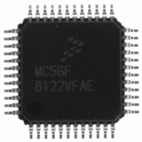
MC56F8122VFAE Freescale Semiconductor, MC56F8122VFAE Datasheet - Page 100

MC56F8122VFAE
Manufacturer Part Number
MC56F8122VFAE
Description
IC DSP 16BIT 40MHZ 48-LQFP
Manufacturer
Freescale Semiconductor
Series
56F8xxxr
Datasheet
1.MC56F8122VFAE.pdf
(136 pages)
Specifications of MC56F8122VFAE
Core Processor
56800
Core Size
16-Bit
Speed
40MHz
Connectivity
SCI, SPI
Peripherals
POR, WDT
Number Of I /o
21
Program Memory Size
32KB (16K x 16)
Program Memory Type
FLASH
Ram Size
4K x 16
Voltage - Supply (vcc/vdd)
2.25 V ~ 3.6 V
Data Converters
A/D 6x12b
Oscillator Type
Internal
Operating Temperature
-40°C ~ 105°C
Package / Case
48-LQFP
Data Bus Width
16 bit
Processor Series
MC56F81xx
Core
56800E
Maximum Clock Frequency
40 MHz
Number Of Programmable I/os
21
Data Ram Size
8 KB
Operating Supply Voltage
- 0.3 V to + 4 V
Maximum Operating Temperature
+ 105 C
Mounting Style
SMD/SMT
Data Rom Size
8 KB
Minimum Operating Temperature
- 40 C
Lead Free Status / RoHS Status
Lead free / RoHS Compliant
Eeprom Size
-
Lead Free Status / Rohs Status
Lead free / RoHS Compliant
Available stocks
Company
Part Number
Manufacturer
Quantity
Price
Company:
Part Number:
MC56F8122VFAE
Manufacturer:
Freescale Semiconductor
Quantity:
10 000
8.3 Memory Maps
The width of the GPIO port defines how many bits are implemented in each of the GPIO registers. Based
on this and the default function of each of the GPIO pins, the reset values of the GPIOx_PUR and
GPIOx_PER registers change from port to port. Tables
these registers.
Part 9 Joint Test Action Group (JTAG)
9.1 JTAG Information
Please
device/package-specific BSDL information.
The TRST pin is not available in this package. The pin is tied to V
The JTAG state machine is reset during POR and can also be reset via a soft reset by holding TMS high
for five rising edges of TCK, as described in the 56F8300 Peripheral User Manual.
100
GPIO Function
GPIOB7
GPIOC0
GPIOC1
GPIOC2
GPIOC3
GPIOC4
GPIOC5
GPIOC6
contact
PHASEA0 / TA0
EXTAL
XTAL
CAN_RX
CAN_TX
TC3
TC1 / RXD0
TC0 / TXD0
Peripheral Function
your
Table 8-3 GPIO External Signals Map (Continued)
Pins in shaded rows are not available in 56F8322 / 56F8122
Pins in italics are NOT available in the 56F8122 device
Freescale
56F8322 Techncial Data, Rev. 16
marketing
Package Pin
38
32
33
46
47
48
1
representative
4-21
Quad Decoder 0 register DECCR is used to select
between Decoder 0 and Timer A
Quad Dec is NOT available in 56F8122
Pull-ups should default to disabled
Pull-ups should default to disabled
CAN is NOT available in 56F8122
CAN is NOT available in 56F8122
SIM register SIM_GPS is used to select between Timer C
and SCI0 on a pin-by-pin basis
SIM register SIM_GPS is used to select between Timer C
and SCI0 on a pin-by-pin basis
through
DD
4-23
or
in the package.
define the actual reset values of
authorized
Notes
Freescale Semiconductor
distributor
Preliminary
for


