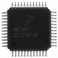
MC56F8122VFAE Freescale Semiconductor, MC56F8122VFAE Datasheet - Page 86

MC56F8122VFAE
Manufacturer Part Number
MC56F8122VFAE
Description
IC DSP 16BIT 40MHZ 48-LQFP
Manufacturer
Freescale Semiconductor
Series
56F8xxxr
Datasheet
1.MC56F8122VFAE.pdf
(136 pages)
Specifications of MC56F8122VFAE
Core Processor
56800
Core Size
16-Bit
Speed
40MHz
Connectivity
SCI, SPI
Peripherals
POR, WDT
Number Of I /o
21
Program Memory Size
32KB (16K x 16)
Program Memory Type
FLASH
Ram Size
4K x 16
Voltage - Supply (vcc/vdd)
2.25 V ~ 3.6 V
Data Converters
A/D 6x12b
Oscillator Type
Internal
Operating Temperature
-40°C ~ 105°C
Package / Case
48-LQFP
Data Bus Width
16 bit
Processor Series
MC56F81xx
Core
56800E
Maximum Clock Frequency
40 MHz
Number Of Programmable I/os
21
Data Ram Size
8 KB
Operating Supply Voltage
- 0.3 V to + 4 V
Maximum Operating Temperature
+ 105 C
Mounting Style
SMD/SMT
Data Rom Size
8 KB
Minimum Operating Temperature
- 40 C
Lead Free Status / RoHS Status
Lead free / RoHS Compliant
Eeprom Size
-
Lead Free Status / Rohs Status
Lead free / RoHS Compliant
Available stocks
Company
Part Number
Manufacturer
Quantity
Price
Company:
Part Number:
MC56F8122VFAE
Manufacturer:
Freescale Semiconductor
Quantity:
10 000
6.5.6.3
This bit controls the pull-up resistors on the IRQA pin.
6.5.6.4
This bit field is reserved or not implemented. It is read as 0 and cannot be modified by writing.
6.5.6.5
This bit controls the pull-up resistors on the TRST (This pin is always tied inactive on the 56F8322), TMS
and TDI pins.
6.5.6.6
This bit field is reserved or not implemented. It is read as 0 and cannot be modified by writing.
6.5.7
The CLKO select register can be used to multiplex out any one of the clocks generated inside the clock
generation and SIM modules. The default value is SYS_CLK. All other clocks primarily muxed out are
for test purposes only, and are subject to significant unspecified latencies at high frequencies.
The upper four bits of the GPIOB register can function as GPIO, Quad Decoder #0 signals, or as additional
clock output signals. GPIO has priority and is enabled/disabled via the GPIOB_PER. If GPIOB[7:4] are
programmed to operate as peripheral outputs, then the choice between Quad Decoder #0 and additional
clock outputs is made here in the CLKOSR. The default state is for the peripheral function of GPIOB[7:4]
to be programmed as Quad Decoder #0. This can be changed by altering PHASE0 through INDEX as
shown in
The CLKOUT pin is not bonded out in this device. Instead, it is offered only as a pad for die-level testing.
6.5.7.1
This bit field is reserved or not implemented. It is read as 0 and cannot be modified by writing.
6.5.7.2
6.5.7.3
86
•
•
•
•
Base + $A
RESET
0 = Peripheral output function of GPIOB[7] is defined to be PHASEA0
1 = Peripheral output function of GPI B[7] is defined to be the oscillator clock (MSTR_OSC, see
Figure
0 = Peripheral output function of GPIOB[6] is defined to be PHASEB0
1 = Peripheral output function of GPIOB[6] is defined to be SYS_CLK2
Read
Write
Figure
CLKO Select Register (SIM_CLKOSR)
IRQ—Bit 10
Reserved—Bits 9–4
JTAG—Bit 3
Reserved—Bits 2–0
Reserved—Bits 15–10
PHASEA0 (PHSA)—Bit 9
PHASEB0 (PHSB)—Bit 8
3-4)
6-9.
15
0
0
14
0
0
Figure 6-9 CLKO Select Register (SIM_CLKOSR)
13
0
0
12
0
0
56F8322 Techncial Data, Rev. 16
11
0
0
10
0
0
PHSA PHSB INDEX HOME
9
0
8
0
7
0
6
0
CLK
DIS
5
1
4
0
3
0
Freescale Semiconductor
CLKOSEL
2
0
1
0
Preliminary
0
0


