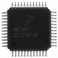
MC56F8122VFAE Freescale Semiconductor, MC56F8122VFAE Datasheet - Page 27

MC56F8122VFAE
Manufacturer Part Number
MC56F8122VFAE
Description
IC DSP 16BIT 40MHZ 48-LQFP
Manufacturer
Freescale Semiconductor
Series
56F8xxxr
Datasheet
1.MC56F8122VFAE.pdf
(136 pages)
Specifications of MC56F8122VFAE
Core Processor
56800
Core Size
16-Bit
Speed
40MHz
Connectivity
SCI, SPI
Peripherals
POR, WDT
Number Of I /o
21
Program Memory Size
32KB (16K x 16)
Program Memory Type
FLASH
Ram Size
4K x 16
Voltage - Supply (vcc/vdd)
2.25 V ~ 3.6 V
Data Converters
A/D 6x12b
Oscillator Type
Internal
Operating Temperature
-40°C ~ 105°C
Package / Case
48-LQFP
Data Bus Width
16 bit
Processor Series
MC56F81xx
Core
56800E
Maximum Clock Frequency
40 MHz
Number Of Programmable I/os
21
Data Ram Size
8 KB
Operating Supply Voltage
- 0.3 V to + 4 V
Maximum Operating Temperature
+ 105 C
Mounting Style
SMD/SMT
Data Rom Size
8 KB
Minimum Operating Temperature
- 40 C
Lead Free Status / RoHS Status
Lead free / RoHS Compliant
Eeprom Size
-
Lead Free Status / Rohs Status
Lead free / RoHS Compliant
Available stocks
Company
Part Number
Manufacturer
Quantity
Price
Company:
Part Number:
MC56F8122VFAE
Manufacturer:
Freescale Semiconductor
Quantity:
10 000
Freescale Semiconductor
Preliminary
Signal Name
(GPIOC5)
(RXD0)
RESET
IRQA
(V
TC1
PP
Table 2-2 Signal and Package Information for the 48-Pin LQFP (Continued)
)
Pin No.
48
11
2
Schmitt
Schmitt
Schmitt
Schmitt
Output
Output
Output
Input/
Input/
Type
Input
Input
State During
enabled
enabled
enabled
pull-up
pull-up
pull-up
Reset
Input,
Input,
Input,
56F8322 Technical Data, Rev. 16
TC1 — Timer C, Channel 1
Receive Data — SCI0 receive data input
Port C GPIO — This GPIO pin can be individually programmed as an
input or output pin.
After reset, the default state is TC1.
External Interrupt Request A — The IRQA input is an asynchronous
external interrupt request during Stop and Wait mode operation.
During other operating modes, it is a synchronized external interrupt
request which indicates an external device is requesting service. It
can be programmed to be level-sensitive or negative-edge-triggered.
V
Reset — This input is a direct hardware reset on the processor. When
RESET is asserted low, the hybrid controller is initialized and placed
in the reset state. A Schmitt trigger input is used for noise immunity.
The internal reset signal will be deasserted synchronous with the
internal clocks after a fixed number of internal clocks.
To ensure complete hardware reset, RESET and TRST should be
asserted together. The only exception occurs in a debugging
environment when a hardware DSP reset is required and it is
necessary not to reset the JTAG/EOnCE module. In this case, assert
RESET, but do not assert TRST.
PP
— This pin is used for Flash debugging purposes.
Signal Description
Signal Pins
27


