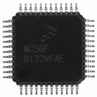
MC56F8122VFAE Freescale Semiconductor, MC56F8122VFAE Datasheet - Page 91

MC56F8122VFAE
Manufacturer Part Number
MC56F8122VFAE
Description
IC DSP 16BIT 40MHZ 48-LQFP
Manufacturer
Freescale Semiconductor
Series
56F8xxxr
Datasheet
1.MC56F8122VFAE.pdf
(136 pages)
Specifications of MC56F8122VFAE
Core Processor
56800
Core Size
16-Bit
Speed
40MHz
Connectivity
SCI, SPI
Peripherals
POR, WDT
Number Of I /o
21
Program Memory Size
32KB (16K x 16)
Program Memory Type
FLASH
Ram Size
4K x 16
Voltage - Supply (vcc/vdd)
2.25 V ~ 3.6 V
Data Converters
A/D 6x12b
Oscillator Type
Internal
Operating Temperature
-40°C ~ 105°C
Package / Case
48-LQFP
Data Bus Width
16 bit
Processor Series
MC56F81xx
Core
56800E
Maximum Clock Frequency
40 MHz
Number Of Programmable I/os
21
Data Ram Size
8 KB
Operating Supply Voltage
- 0.3 V to + 4 V
Maximum Operating Temperature
+ 105 C
Mounting Style
SMD/SMT
Data Rom Size
8 KB
Minimum Operating Temperature
- 40 C
Lead Free Status / RoHS Status
Lead free / RoHS Compliant
Eeprom Size
-
Lead Free Status / Rohs Status
Lead free / RoHS Compliant
Available stocks
Company
Part Number
Manufacturer
Quantity
Price
Company:
Part Number:
MC56F8122VFAE
Manufacturer:
Freescale Semiconductor
Quantity:
10 000
6.5.9.10
Each bit controls clocks to the indicated peripheral.
6.5.9.11
Each bit controls clocks to the indicated peripheral.
6.5.9.12
Each bit controls clocks to the indicated peripheral.
6.5.9.13
Each bit controls clocks to the indicated peripheral.
6.5.9.14
This bit field is reserved or not implemented. It is read as 1 and cannot be modified by writing.
6.5.9.15
Each bit controls clocks to the indicated peripheral.
6.5.10
The I/O Short Address Location registers are used to specify the memory referenced via the I/O short
address mode. The I/O short address mode allows the instruction to specify the lower six bits of address;
the upper address bits are not directly controllable. This register set allows limited control of the full
address, as shown in
Note:
Freescale Semiconductor
Preliminary
•
•
•
•
•
•
•
•
•
•
1 = Clocks are enabled
0 = The clock is not provided to the peripheral (the peripheral is disabled)
1 = Clocks are enabled
0 = The clock is not provided to the peripheral (the peripheral is disabled)
1 = Clocks are enabled
0 = The clock is not provided to the peripheral (the peripheral is disabled)
1 = Clocks are enabled
0 = The clock is not provided to the peripheral (the peripheral is disabled)
1 = Clocks are enabled
0 = The clock is not provided to the peripheral (the peripheral is disabled)
I/O Short Address Location Register (SIM_ISALH and SIM_ISALL)
If this register is set to something other than the top of memory (EOnCE register space) and the EX bit
in the OMR is set to 1, the JTAG port cannot access the on-chip EOnCE registers, and debug functions
will be affected.
Serial Communications Interface 1 Enable (SCI1)—Bit 5
Serial Communications Interface 0 Enable (SCI0)—Bit 4
Serial Peripheral Interface 1 Enable (SPI1)—Bit 3
Serial Peripheral Interface 0 Enable (SPI0)—Bit 2
Reserved—Bit 1
Pulse Width Modulator A Enable (PWMA)—Bit 0
Figure
6-13.
56F8322 Technical Data, Rev. 16
Register Descriptions
91


