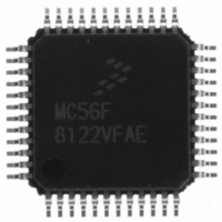
MC56F8122VFAE Freescale Semiconductor, MC56F8122VFAE Datasheet - Page 16

MC56F8122VFAE
Manufacturer Part Number
MC56F8122VFAE
Description
IC DSP 16BIT 40MHZ 48-LQFP
Manufacturer
Freescale Semiconductor
Series
56F8xxxr
Datasheet
1.MC56F8122VFAE.pdf
(136 pages)
Specifications of MC56F8122VFAE
Core Processor
56800
Core Size
16-Bit
Speed
40MHz
Connectivity
SCI, SPI
Peripherals
POR, WDT
Number Of I /o
21
Program Memory Size
32KB (16K x 16)
Program Memory Type
FLASH
Ram Size
4K x 16
Voltage - Supply (vcc/vdd)
2.25 V ~ 3.6 V
Data Converters
A/D 6x12b
Oscillator Type
Internal
Operating Temperature
-40°C ~ 105°C
Package / Case
48-LQFP
Data Bus Width
16 bit
Processor Series
MC56F81xx
Core
56800E
Maximum Clock Frequency
40 MHz
Number Of Programmable I/os
21
Data Ram Size
8 KB
Operating Supply Voltage
- 0.3 V to + 4 V
Maximum Operating Temperature
+ 105 C
Mounting Style
SMD/SMT
Data Rom Size
8 KB
Minimum Operating Temperature
- 40 C
Lead Free Status / RoHS Status
Lead free / RoHS Compliant
Eeprom Size
-
Lead Free Status / Rohs Status
Lead free / RoHS Compliant
Available stocks
Company
Part Number
Manufacturer
Quantity
Price
Company:
Part Number:
MC56F8122VFAE
Manufacturer:
Freescale Semiconductor
Quantity:
10 000
Part 2 Signal/Connection Descriptions
2.1 Introduction
The input and output signals of the 56F8322 and 56F8122 devices are organized into functional groups,
as detailed in
describes the signal or signals present on a pin.
Note: See
16
1. The V
2. Pins in this section can function as SPI #1 and GPIO.
3. Pins in this section can function as SCI #1 and GPIO.
4. Alternately, can function as Quad Timer A pins or GPIO.
5. Pins can function as SCI #0 and GPIO.
6. Tied internally to ANA7
Power (V
Ground (V
Supply Capacitors & V
PLL and Clock
Interrupt and Program Control
Pulse Width Modulator (PWM) Ports
Serial Peripheral Interface (SPI) Port 0
Quadrature Decoder Port 0
CAN Ports
Analog to Digital Converter (ADC) Ports
Timer Module Port C
Timer Module Port A
JTAG/Enhanced On-Chip Emulation (EOnCE)
Temperature Sense
Dedicated GPIO
Table 1-1
PP
Table 2-1
DD
input shares the IRQA input
SS
for 56F8122 functional differences.
or V
or V
DDA
SSA
Functional Group
6
)
5
)
and as illustrated in
PP
Table 2-1 Functional Group Pin Allocations
1
4
2
56F8322 Techncial Data, Rev. 16
3
Figure 2-1
and
Figure
56F8322
—
—
Number of Pins in Package
5
5
2
2
2
7
4
4
2
9
2
4
0
2-2. In
Table
2-2, each table row
Freescale Semiconductor
56F8122
—
—
—
—
5
5
2
2
2
8
9
2
4
4
5
Preliminary


