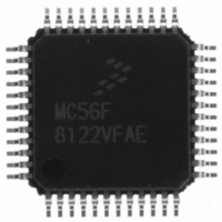
MC56F8122VFAE Freescale Semiconductor, MC56F8122VFAE Datasheet - Page 36

MC56F8122VFAE
Manufacturer Part Number
MC56F8122VFAE
Description
IC DSP 16BIT 40MHZ 48-LQFP
Manufacturer
Freescale Semiconductor
Series
56F8xxxr
Datasheet
1.MC56F8122VFAE.pdf
(136 pages)
Specifications of MC56F8122VFAE
Core Processor
56800
Core Size
16-Bit
Speed
40MHz
Connectivity
SCI, SPI
Peripherals
POR, WDT
Number Of I /o
21
Program Memory Size
32KB (16K x 16)
Program Memory Type
FLASH
Ram Size
4K x 16
Voltage - Supply (vcc/vdd)
2.25 V ~ 3.6 V
Data Converters
A/D 6x12b
Oscillator Type
Internal
Operating Temperature
-40°C ~ 105°C
Package / Case
48-LQFP
Data Bus Width
16 bit
Processor Series
MC56F81xx
Core
56800E
Maximum Clock Frequency
40 MHz
Number Of Programmable I/os
21
Data Ram Size
8 KB
Operating Supply Voltage
- 0.3 V to + 4 V
Maximum Operating Temperature
+ 105 C
Mounting Style
SMD/SMT
Data Rom Size
8 KB
Minimum Operating Temperature
- 40 C
Lead Free Status / RoHS Status
Lead free / RoHS Compliant
Eeprom Size
-
Lead Free Status / Rohs Status
Lead free / RoHS Compliant
Available stocks
Company
Part Number
Manufacturer
Quantity
Price
Company:
Part Number:
MC56F8122VFAE
Manufacturer:
Freescale Semiconductor
Quantity:
10 000
4.4 Data Map
Note: Data Flash is NOT available on the 56F8122 device.
4.5 Flash Memory Map
Figure 4-1
Flash Memory is divided into three functional blocks. The Program and boot memories reside on the
Program Memory buses. They are controlled by one set of banked registers. Data Memory Flash resides
on the Data Memory buses and is controlled separately by its own set of banked registers.
The top nine words of the Program Memory Flash are treated as special memory locations. The content of
these words is used to control the operation of the Flash Controller. Because these words are part of the
Flash Memory content, their state is maintained during power-down and reset. During chip initialization,
the content of these memory locations is loaded into Flash Memory control registers, detailed in the Flash
Memory chapter of the 56F8300 Peripheral User Manual. These configure parameters are located
between $00_3FF7 and $00_3FFF.
36
illustrates the Flash Memory (FM) map on the system bus.
1. All addresses are 16-bit Word addresses.
2. The Data RAM is organized as a 2K x 32-bit memory to allow single-cycle,
X:$FF FFFF
X:$FF FF00
X:$FF FEFF
X:$01 0000
X:$00 FFFF
X:$00 F000
X:$00 EFFF
X:$00 2000
X:$00 1FFF
X:$00 1000
X:$00 0FFF
X:$00 0000
Begin/End Address
long-word operations
Table 4-4 Data Memory Map
56F8322 Techncial Data, Rev. 16
EOnCE
256 locations allocated
RESERVED
On-Chip Peripherals
4096 locations allocated
RESERVED
On-Chip Data Flash
8KB
On-Chip Data RAM
8KB
2
Memory Allocation
1
Freescale Semiconductor
Preliminary


