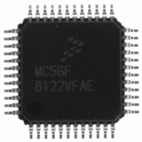
MC56F8122VFAE Freescale Semiconductor, MC56F8122VFAE Datasheet - Page 19

MC56F8122VFAE
Manufacturer Part Number
MC56F8122VFAE
Description
IC DSP 16BIT 40MHZ 48-LQFP
Manufacturer
Freescale Semiconductor
Series
56F8xxxr
Datasheet
1.MC56F8122VFAE.pdf
(136 pages)
Specifications of MC56F8122VFAE
Core Processor
56800
Core Size
16-Bit
Speed
40MHz
Connectivity
SCI, SPI
Peripherals
POR, WDT
Number Of I /o
21
Program Memory Size
32KB (16K x 16)
Program Memory Type
FLASH
Ram Size
4K x 16
Voltage - Supply (vcc/vdd)
2.25 V ~ 3.6 V
Data Converters
A/D 6x12b
Oscillator Type
Internal
Operating Temperature
-40°C ~ 105°C
Package / Case
48-LQFP
Data Bus Width
16 bit
Processor Series
MC56F81xx
Core
56800E
Maximum Clock Frequency
40 MHz
Number Of Programmable I/os
21
Data Ram Size
8 KB
Operating Supply Voltage
- 0.3 V to + 4 V
Maximum Operating Temperature
+ 105 C
Mounting Style
SMD/SMT
Data Rom Size
8 KB
Minimum Operating Temperature
- 40 C
Lead Free Status / RoHS Status
Lead free / RoHS Compliant
Eeprom Size
-
Lead Free Status / Rohs Status
Lead free / RoHS Compliant
Available stocks
Company
Part Number
Manufacturer
Quantity
Price
Company:
Part Number:
MC56F8122VFAE
Manufacturer:
Freescale Semiconductor
Quantity:
10 000
2.2 Signal Pins
After reset, each pin is configured for its primary function (listed first). In the 56F8122, after reset, each
pin must be configured for the desired function. The initialization software will configure each pin for the
function listed first for each pin, as shown in
Note: Signals in italics are not available in the 56F8122 device.
If the “State During Reset” lists more than one state for a pin, the first state is the actual reset state. Other
states show the reset condition of the alternate function, which you get if the alternate pin function is
selected without changing the configuration of the alternate peripheral. For example, the SCLK0/GPIOB3
pin shows that it is tri-stated during reset. If the GPIOB_PER is changed to select the GPIO function of
the pin, it will become an input if no other registers are changed.
Freescale Semiconductor
Preliminary
Signal Name
V
V
DDA_ADC
SSA_ADC
V
V
V
V
V
V
DD_IO
DD_IO
DD_IO
DD_IO
V
V
V
V
CAP
CAP
SS
SS
SS
SS
1
2
Table 2-2 Signal and Package Information for the 48-Pin LQFP
Pin No.
14
34
44
30
10
13
31
45
29
43
17
5
Supply
Supply
Supply
Supply
Supply
Type
State During
Supply
Reset
56F8322 Technical Data, Rev. 16
Table
I/O Power — This pin supplies 3.3V power to the chip I/O interface
and also the Processor core throught the on-chip voltage regulator, if
it is enabled.
ADC Power — This pin supplies 3.3V power to the ADC modules. It
must be connected to a clean analog power supply.
Ground — These pins provide ground for chip logic and I/O drivers.
ADC Analog Ground — This pin supplies an analog ground to the
ADC modules.
V
in order to bypass the core logic voltage regulator, required for proper
chip operation.
CAP
1 - 2 — Connect each pin to a 2.2μF or greater bypass capacitor
2-2. Any alternate functionality must be programmed.
Signal Description
Signal Pins
19


