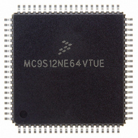
MC9S12NE64VTUE Freescale Semiconductor, MC9S12NE64VTUE Datasheet - Page 57

MC9S12NE64VTUE
Manufacturer Part Number
MC9S12NE64VTUE
Description
IC MCU 64K FLASH EEPROM 80-TQFP
Manufacturer
Freescale Semiconductor
Series
HCS12r
Datasheet
1.MC9S12NE64VTU.pdf
(554 pages)
Specifications of MC9S12NE64VTUE
Core Processor
HCS12
Core Size
16-Bit
Speed
25MHz
Connectivity
EBI/EMI, Ethernet, I²C, SCI, SPI
Peripherals
POR, PWM, WDT
Number Of I /o
38
Program Memory Size
64KB (64K x 8)
Program Memory Type
FLASH
Ram Size
8K x 8
Voltage - Supply (vcc/vdd)
2.375 V ~ 3.465 V
Data Converters
A/D 8x10b
Oscillator Type
Internal
Operating Temperature
-40°C ~ 105°C
Package / Case
80-TQFP Exposed Pad, 80-eTQFP, 80-HTQFP, 80-VQFP
Processor Series
S12N
Core
HCS12
Data Bus Width
16 bit
Data Ram Size
8 KB
Interface Type
I2C, SCI, SPI
Maximum Clock Frequency
125 MHz
Number Of Programmable I/os
70
Number Of Timers
4
Operating Supply Voltage
- 0.3 V to + 3 V
Maximum Operating Temperature
+ 105 C
Mounting Style
SMD/SMT
3rd Party Development Tools
EWHCS12
Development Tools By Supplier
EVB9S12NE64E, DEMO9S12NE64E
Minimum Operating Temperature
- 65 C
On-chip Adc
10 bit, 8 Channel
Cpu Family
HCS12
Device Core Size
16b
Frequency (max)
25MHz
Total Internal Ram Size
8KB
# I/os (max)
70
Number Of Timers - General Purpose
4
Operating Supply Voltage (typ)
2.5/3.3V
Operating Supply Voltage (max)
2.625/3.465V
Operating Supply Voltage (min)
2.357/2.375/3.135V
Instruction Set Architecture
CISC
Operating Temp Range
-40C to 105C
Operating Temperature Classification
Industrial
Mounting
Surface Mount
Pin Count
80
Package Type
TQFP
For Use With
EVB9S12NE64E - BOARD EVAL FOR 9S12NE64DEMO9S12NE64E - DEMO BOARD FOR 9S12NE64
Lead Free Status / RoHS Status
Lead free / RoHS Compliant
Eeprom Size
-
Lead Free Status / Rohs Status
Lead free / RoHS Compliant
Available stocks
Company
Part Number
Manufacturer
Quantity
Price
Company:
Part Number:
MC9S12NE64VTUE
Manufacturer:
Freescale Semiconductor
Quantity:
10 000
Part Number:
MC9S12NE64VTUE
Manufacturer:
FREESCALE
Quantity:
20 000
- Current page: 57 of 554
- Download datasheet (4Mb)
1.2.3.60 PHY_RBIAS — EPHY Bias Control Resistor
Connect a 1.0% external resistor, RBIAS, between PHY_RBIAS pin and PHY_VSSA. This resistor must
be placed as near as possible to the chip pin. Stray capacitance must be kept to less than 10 pF (> 50 pF
may cause instability). No high-speed signals are allowed in the region of RBIAS.
1.2.4
1.2.4.1
External power and ground for I/O drivers. Bypass requirements depend on how heavily the MCU pins are
loaded.
1.2.4.2
External power for internal voltage regulator.
1.2.4.3
Power is supplied to the MCU through VDD and VSS. This 2.5V supply is derived from the internal
voltage regulator. No static load is allowed on these pins. The internal voltage regulator is turned off, if
VDDR/VREGEN is tied to ground.
1.2.4.4
VDDA and VSSA are the power supply and ground input pins for the voltage regulator and the
analog-to-digital converter.
1.2.4.5
Power is supplied to the Ethernet physical transceiver (EPHY) PLLs through PHY_VDDA and
PHY_VSSA. This 2.5V supply is derived from the internal voltage regulator. No static load is allowed on
these pins. The internal voltage regulator is turned off, if VDDR/VREGEN is tied to ground.
1.2.4.6
Power is supplied to the Ethernet physical transceiver (EPHY) receiver through PHY_VDDRX and
PHY_VSSRX. This 2.5V supply is derived from the internal voltage regulator. No static load is allowed
on these pins. The internal voltage regulator is turned off, if VDDR/VREGEN is tied to ground.
1.2.4.7
External power is supplied to the Ethernet physical transceiver (EPHY) transmitter through PHY_VDDTX
and PHY_VSSTX. This 2.5 V supply is derived from the internal voltage regulator. No static load is
allowed on these pins. The internal voltage regulator is turned off, if V
Freescale Semiconductor
Power Supply Pins
V
Voltage Regulator
V
V
V
PHY_VDDA, PHY_VSSA — Power Supply Pins for EPHY Analog
PHY_VDDRX, PHY_VSSRX — Power Supply Pins for EPHY Receiver
PHY_VDDTX, PHY_VSSTX — Power Supply Pins for EPHY Transmitter
DDX1
DDR
DD1
DDA
, V
/V
, V
, V
REGEN
DD2
SSA
DDX2
, V
— Power Supply Pins for ATD and VREG_PHY
, V
SS1
— Power Pin for Internal Voltage Regulator
SSX1
, V
SS2
MC9S12NE64 Data Sheet, Rev 1.0
, V
SSX2
— Core Power Pins
— Power & Ground Pins for I/O & Internal
DDR
/V
REGEN
is tied to ground.
Signal Description
57
Related parts for MC9S12NE64VTUE
Image
Part Number
Description
Manufacturer
Datasheet
Request
R
Part Number:
Description:
Manufacturer:
Freescale Semiconductor, Inc
Datasheet:
Part Number:
Description:
Manufacturer:
Freescale Semiconductor, Inc
Datasheet:
Part Number:
Description:
Manufacturer:
Freescale Semiconductor, Inc
Datasheet:
Part Number:
Description:
Manufacturer:
Freescale Semiconductor, Inc
Datasheet:
Part Number:
Description:
Manufacturer:
Freescale Semiconductor, Inc
Datasheet:
Part Number:
Description:
Manufacturer:
Freescale Semiconductor, Inc
Datasheet:
Part Number:
Description:
Manufacturer:
Freescale Semiconductor, Inc
Datasheet:
Part Number:
Description:
Manufacturer:
Freescale Semiconductor, Inc
Datasheet:
Part Number:
Description:
Manufacturer:
Freescale Semiconductor, Inc
Datasheet:
Part Number:
Description:
Manufacturer:
Freescale Semiconductor, Inc
Datasheet:
Part Number:
Description:
Manufacturer:
Freescale Semiconductor, Inc
Datasheet:
Part Number:
Description:
Manufacturer:
Freescale Semiconductor, Inc
Datasheet:
Part Number:
Description:
Manufacturer:
Freescale Semiconductor, Inc
Datasheet:
Part Number:
Description:
Manufacturer:
Freescale Semiconductor, Inc
Datasheet:
Part Number:
Description:
Manufacturer:
Freescale Semiconductor, Inc
Datasheet:


