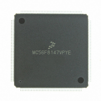
MC56F8147VPYE Freescale Semiconductor, MC56F8147VPYE Datasheet - Page 109

MC56F8147VPYE
Manufacturer Part Number
MC56F8147VPYE
Description
IC DSP 16BIT 40MHZ 160-LQFP
Manufacturer
Freescale Semiconductor
Series
56F8xxxr
Datasheet
1.MC56F8147VPYE.pdf
(172 pages)
Specifications of MC56F8147VPYE
Core Processor
56800
Core Size
16-Bit
Speed
40MHz
Connectivity
EBI/EMI, SCI, SPI
Peripherals
POR, PWM, WDT
Number Of I /o
76
Program Memory Size
128KB (64K x 16)
Program Memory Type
FLASH
Ram Size
4K x 16
Voltage - Supply (vcc/vdd)
2.25 V ~ 3.6 V
Data Converters
A/D 16x12b
Oscillator Type
External
Operating Temperature
-40°C ~ 105°C
Package / Case
160-LQFP
Data Bus Width
16 bit
Processor Series
MC56F81xx
Core
56800E
Data Ram Size
4 KB
Interface Type
SPI, SCI, CAN
Maximum Clock Frequency
40 MHz
Number Of Programmable I/os
76
Number Of Timers
2
Maximum Operating Temperature
+ 105 C
Mounting Style
SMD/SMT
Minimum Operating Temperature
- 40 C
On-chip Adc
4 x 12 bit, 4 Channel
Lead Free Status / RoHS Status
Lead free / RoHS Compliant
Eeprom Size
-
Lead Free Status / Rohs Status
Lead free / RoHS Compliant
Available stocks
Company
Part Number
Manufacturer
Quantity
Price
Company:
Part Number:
MC56F8147VPYE
Manufacturer:
FREESCAL
Quantity:
253
Company:
Part Number:
MC56F8147VPYE
Manufacturer:
Freescale Semiconductor
Quantity:
10 000
6.5.3.1
This register is reset only by the Power-On Reset (POR). It has no part-specific functionality and is
intended for use by a software developer to contain data that will be unaffected by the other reset sources
(RESET pin, software reset, and COP reset).
6.5.4
This read-only register displays the most significant half of the JTAG ID for the chip. This register reads
$11F4.
6.5.5
This read-only register displays the least significant half of the JTAG ID for the chip. This register reads
$401D.
6.5.6
Most of the pins on the chip have on-chip pull-up resistors. Pins which can operate as GPIO can have these
resistors disabled via the GPIO function. Non-GPIO pins can have their pull-ups disabled by setting the
appropriate bit in this register. Disabling pull-ups is done on a peripheral-by-peripheral basis (for pins not
muxed with GPIO). Each bit in the register (see
Table 2-2
Freescale Semiconductor
Preliminary
Base + $8
RESET
Write
Read
Base + $6
Base + $7
RESET
RESET
Read
Write
Read
Write
to identify which pins can deactivate the internal pull-up resistor.
Most Significant Half of JTAG ID (SIM_MSH_ID)
Least Significant Half of JTAG ID (SIM_LSH_ID)
SIM Pull-up Disable Register (SIM_PUDR)
Software Control Data 1 (FIELD)—Bits 15–0
15
0
0
15
15
PWMA1
Figure 6-6 Most Significant Half of JTAG ID (SIM_MSH_ID)
Figure 6-7 Least Significant Half of JTAG ID (SIM_LSH_ID)
0
0
0
0
14
0
Figure 6-8 SIM Pull-up Disable Register (SIM_PUDR)
14
14
0
0
1
1
CAN
13
0
13
13
0
0
0
0
MODE
EMI_
12
0
12
12
0
0
0
0
RESET
11
0
56F8347 Technical Data, Rev.11
11
11
0
0
0
0
IRQ
10
0
10
10
0
0
0
0
XBOOT PWMB PWMA0
Figure
9
0
9
0
0
9
0
0
6-8) corresponds to a functional group of pins. See
8
0
8
8
1
1
0
0
7
0
7
7
1
1
0
0
6
6
1
1
0
0
6
0
0
CTRL
5
1
1
5
0
0
5
0
4
1
1
4
1
1
4
0
0
JTAG
3
3
3
0
0
0
1
1
2
1
1
2
1
1
2
0
0
Register Descriptions
1
0
0
1
0
0
1
0
0
0
0
0
0
1
1
0
0
0
109


