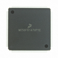
MC56F8147VPYE Freescale Semiconductor, MC56F8147VPYE Datasheet - Page 140

MC56F8147VPYE
Manufacturer Part Number
MC56F8147VPYE
Description
IC DSP 16BIT 40MHZ 160-LQFP
Manufacturer
Freescale Semiconductor
Series
56F8xxxr
Datasheet
1.MC56F8147VPYE.pdf
(172 pages)
Specifications of MC56F8147VPYE
Core Processor
56800
Core Size
16-Bit
Speed
40MHz
Connectivity
EBI/EMI, SCI, SPI
Peripherals
POR, PWM, WDT
Number Of I /o
76
Program Memory Size
128KB (64K x 16)
Program Memory Type
FLASH
Ram Size
4K x 16
Voltage - Supply (vcc/vdd)
2.25 V ~ 3.6 V
Data Converters
A/D 16x12b
Oscillator Type
External
Operating Temperature
-40°C ~ 105°C
Package / Case
160-LQFP
Data Bus Width
16 bit
Processor Series
MC56F81xx
Core
56800E
Data Ram Size
4 KB
Interface Type
SPI, SCI, CAN
Maximum Clock Frequency
40 MHz
Number Of Programmable I/os
76
Number Of Timers
2
Maximum Operating Temperature
+ 105 C
Mounting Style
SMD/SMT
Minimum Operating Temperature
- 40 C
On-chip Adc
4 x 12 bit, 4 Channel
Lead Free Status / RoHS Status
Lead free / RoHS Compliant
Eeprom Size
-
Lead Free Status / Rohs Status
Lead free / RoHS Compliant
Available stocks
Company
Part Number
Manufacturer
Quantity
Price
Company:
Part Number:
MC56F8147VPYE
Manufacturer:
FREESCAL
Quantity:
253
Company:
Part Number:
MC56F8147VPYE
Manufacturer:
Freescale Semiconductor
Quantity:
10 000
1. N/A, since device captures data before it deasserts RD
2. If RWSS = RWSH = 0, and the chip select does not change, then RD does not deassert during back-to-back reads.
3. Substitute BMDAR for MDAR if there is no chip select
4. MDAR is active in this calculation only when the chip select changes.
140
Address Valid to WR Asserted
WR Width Asserted to WR
Deasserted
Valid Data Out Hold Time after WR
Deasserted
Valid Data Out Set-Up Time to WR
Deasserted
Valid Address after WR Deasserted
RD Deasserted to Address Invalid
Address Valid to RD Deasserted
Valid Input Data Hold after RD
Deasserted
RD Assertion Width
Address Valid to Input Data Valid
Address Valid to RD Asserted
RD Asserted to Input Data Valid
WR Deasserted to RD Asserted
RD Deasserted to RD Asserted
WR Deasserted to WR Asserted
RD Deasserted to WR Asserted
Data Out Valid to WR Asserted
Characteristic
Table 10-16 External Memory Interface Timing
Symbol
t
t
t
t
t
t
WRWR
WRRD
RDWR
t
t
t
t
t
t
ARDD
t
ARDA
t
RDRD
AWR
t
DWR
WAC
DOH
DOS
DRD
t
RDD
RDA
t
WR
RD
AD
56F8347 Technical Data, Rev.11
Configuration
Wait States
WWS=0
WWS>0
WWS=0
WWS>0
WWS=0
WWS=0
WWS>0
WWS>0
WWS=0
WWS>0
WWS=0
WWS>0
-10.252
-14.414
-19.299
-12.411
-17.297
-0.357
-2.121
-1.805
-0.063
-0.253
-2.868
-9.505
-2.552
-1.512
-2.047
-9.000
-3.888
-2.922
-1.645
-2.002
-1.323
-1.442
-0.695
-0.476
-0.160
0.257
0.00
D
2
0.75 + DCAOE
0.25 + DCAOE
0.25 + DCAEO
0.25 + DCAOE
0.25 + DCAEO
0.25 + DCAOE
0.25 + DCAEO
1.25 + DCAOE
1.25 + DCAOE
0.25 + DCAEO
0.75 + DCAEO
0.75 + DCAOE
N/A
0.50
0.00
0.50
0.50
0.00
1.00
1.00
1.00
0.00
1.00
0.00
1.00
0.50
M
0
1
Freescale Semiconductor
WWSS, WWSH
RWSH, WWSS,
WWSH,RWSS
RWSS,RWSH
Wait States
WWS,WWSS
RWSS,RWS
RWSS,RWS
RWSS,RWS
Controls
MDAR
MDAR
WWSS
WWSS
WWSH
WWSH
RWSH
RWSS
WWS
RWS
—
3, 4
3
Preliminary
Unit
ns
ns
ns
ns
ns
ns
ns
ns
ns
ns
ns
ns
ns
ns
ns
ns
ns


