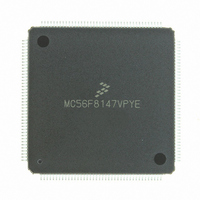
MC56F8147VPYE Freescale Semiconductor, MC56F8147VPYE Datasheet - Page 29

MC56F8147VPYE
Manufacturer Part Number
MC56F8147VPYE
Description
IC DSP 16BIT 40MHZ 160-LQFP
Manufacturer
Freescale Semiconductor
Series
56F8xxxr
Datasheet
1.MC56F8147VPYE.pdf
(172 pages)
Specifications of MC56F8147VPYE
Core Processor
56800
Core Size
16-Bit
Speed
40MHz
Connectivity
EBI/EMI, SCI, SPI
Peripherals
POR, PWM, WDT
Number Of I /o
76
Program Memory Size
128KB (64K x 16)
Program Memory Type
FLASH
Ram Size
4K x 16
Voltage - Supply (vcc/vdd)
2.25 V ~ 3.6 V
Data Converters
A/D 16x12b
Oscillator Type
External
Operating Temperature
-40°C ~ 105°C
Package / Case
160-LQFP
Data Bus Width
16 bit
Processor Series
MC56F81xx
Core
56800E
Data Ram Size
4 KB
Interface Type
SPI, SCI, CAN
Maximum Clock Frequency
40 MHz
Number Of Programmable I/os
76
Number Of Timers
2
Maximum Operating Temperature
+ 105 C
Mounting Style
SMD/SMT
Minimum Operating Temperature
- 40 C
On-chip Adc
4 x 12 bit, 4 Channel
Lead Free Status / RoHS Status
Lead free / RoHS Compliant
Eeprom Size
-
Lead Free Status / Rohs Status
Lead free / RoHS Compliant
Available stocks
Company
Part Number
Manufacturer
Quantity
Price
Company:
Part Number:
MC56F8147VPYE
Manufacturer:
FREESCAL
Quantity:
253
Company:
Part Number:
MC56F8147VPYE
Manufacturer:
Freescale Semiconductor
Quantity:
10 000
Freescale Semiconductor
Preliminary
Table 2-2 Signal and Package Information for the 160-Pin LQFP and MBGA (Continued)
Signal Name
(GPOPC6)
(GPIOC7)
(GPIOE4)
INDEX0
HOME0
SCLK0
(TA2)
(TA3)
157
158
146
Pin
No.
Ball
No.
A1
B3
A6
Schmitt
Schmitt
Schmitt
Schmitt
Schmitt
Schmitt
Schmitt
Schmitt
Output
Output
Output
Output
Output
Output
Input/
Input/
Input/
Input/
Input/
Input/
Type
Input
Input
56F8347 Technical Data, Rev.11
enabled
enabled
enabled
During
pull-up
pull-up
pull-up
Reset
Input,
Input,
Input,
State
Index — Quadrature Decoder 0, INDEX input
TA2 — Timer A, Channel 2
Port C GPIO — This GPIO pin can be individually
programmed as an input or output pin.
After reset, the default state is INDEX0.
To deactivate the internal pull-up resistor, clear bit 6 of the
GPIOC_PUR register.
Home — Quadrature Decoder 0, HOME input
TA3 — Timer A, Channel 3
Port C GPIO — This GPIO pin can be individually
programmed as an input or output pin.
After reset, the default state is HOME0.
To deactivate the internal pull-up resistor, clear bit 7 of the
GPIOC_PUR register.
SPI 0 Serial Clock — In the master mode, this pin serves as
an output, clocking slaved listeners. In slave mode, this pin
serves as the data clock input.
Port E GPIO — This GPIO pin can be individually
programmed as an input or output pin.
After reset, the default state is SCLK0.
To deactivate the internal pull-up resistor, clear bit 4 in the
GPIOE_PUR register.
Signal Description
Signal Pins
29


