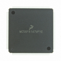
MC56F8147VPYE Freescale Semiconductor, MC56F8147VPYE Datasheet - Page 42

MC56F8147VPYE
Manufacturer Part Number
MC56F8147VPYE
Description
IC DSP 16BIT 40MHZ 160-LQFP
Manufacturer
Freescale Semiconductor
Series
56F8xxxr
Datasheet
1.MC56F8147VPYE.pdf
(172 pages)
Specifications of MC56F8147VPYE
Core Processor
56800
Core Size
16-Bit
Speed
40MHz
Connectivity
EBI/EMI, SCI, SPI
Peripherals
POR, PWM, WDT
Number Of I /o
76
Program Memory Size
128KB (64K x 16)
Program Memory Type
FLASH
Ram Size
4K x 16
Voltage - Supply (vcc/vdd)
2.25 V ~ 3.6 V
Data Converters
A/D 16x12b
Oscillator Type
External
Operating Temperature
-40°C ~ 105°C
Package / Case
160-LQFP
Data Bus Width
16 bit
Processor Series
MC56F81xx
Core
56800E
Data Ram Size
4 KB
Interface Type
SPI, SCI, CAN
Maximum Clock Frequency
40 MHz
Number Of Programmable I/os
76
Number Of Timers
2
Maximum Operating Temperature
+ 105 C
Mounting Style
SMD/SMT
Minimum Operating Temperature
- 40 C
On-chip Adc
4 x 12 bit, 4 Channel
Lead Free Status / RoHS Status
Lead free / RoHS Compliant
Eeprom Size
-
Lead Free Status / Rohs Status
Lead free / RoHS Compliant
Available stocks
Company
Part Number
Manufacturer
Quantity
Price
Company:
Part Number:
MC56F8147VPYE
Manufacturer:
FREESCAL
Quantity:
253
Company:
Part Number:
MC56F8147VPYE
Manufacturer:
Freescale Semiconductor
Quantity:
10 000
4.3 Interrupt Vector Table
Table 4-5
organized with higher-priority vectors at the top and lower-priority interrupts lower in the table. The
priority of an interrupt can be assigned to different levels, as indicated, allowing some control over
interrupt priorities. All level 3 interrupts will be serviced before level 2, and so on. For a selected priority
level, the lowest vector number has the highest priority.
The location of the vector table is determined by the Vector Base Address (VBA) register. Please see
5.6.11
In some configurations, the reset address and COP reset address will correspond to vector 0 and 1 of the
interrupt vector table. In these instances, the first two locations in the vector table must contain branch or
JMP instructions. All other entries must contain JSR instructions.
42
1. If Flash Security Mode is enabled, EXTBOOT Mode 1 cannot be used. See Security Features,
2. This mode provides maximum compatibility with 56F80x parts while operating externally.
3. “EMI_MODE = 0”, EMI_MODE pin is tied to ground at boot up.
4. “EMI_MODE = 1”, EMI_MODE pin is tied to V
5. Not accessible in reset configuration, since the address is above P$0x00 FFFF. The higher bit address/GPIO (and/or chip
6. Booting from this external address allows prototyping of the internal Boot Flash.
7. The internal Program Flash is relocated in this mode, making it accessible.
P:$1F FFFF
P:$10 0000
P:$0F FFFF
P:$03 0000
P:$02 FFFF
P:$02 F800
P:$02 F7FF
P:$02 1000
P:$02 0FFF
P:$02 0000
P:$01 FFFF
P:$01 0000
P:$00 FFFF
P:$00 0000
selects) pins must be reconfigured before this external memory is accessible.
Begin/End
Address
for the reset value of the VBA.
provides the reset and interrupt priority structure, including on-chip peripherals. The table is
External Program Memory
Boot Flash
8KB
COP Reset Address = 02 0002
Boot Location = 02 0000
External Program RAM
Internal Program Flash
128KB
16-Bit External Address Bus
Mode 0 (MA = 0)
Internal Boot
Internal Boot
Table 4-4 Program Memory Map at Reset
5
On-Chip Program RAM
5
56F8347 Technical Data, Rev.11
DD
at boot up.
Reserved
116KB
4KB
External Program Memory
Boot Flash
8KB
(Not Used for Boot in this Mode)
Internal Program Flash
128KB
External Program RAM
COP Reset Address = 00 0002
Boot Location = 00 0000
16-Bit External Address Bus
EMI_MODE = 0
7
2
Mode 1
,
3
5
External Boot
1
(MA = 1)
External Program Memory
External Program RAM
COP Reset Address = 02 0002
Boot Location = 02 0000
20-Bit External Address Bus
Part
7.
EMI_MODE = 1
Freescale Semiconductor
Preliminary
4
6
5
Part


