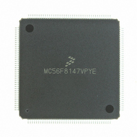
MC56F8147VPYE Freescale Semiconductor, MC56F8147VPYE Datasheet - Page 19

MC56F8147VPYE
Manufacturer Part Number
MC56F8147VPYE
Description
IC DSP 16BIT 40MHZ 160-LQFP
Manufacturer
Freescale Semiconductor
Series
56F8xxxr
Datasheet
1.MC56F8147VPYE.pdf
(172 pages)
Specifications of MC56F8147VPYE
Core Processor
56800
Core Size
16-Bit
Speed
40MHz
Connectivity
EBI/EMI, SCI, SPI
Peripherals
POR, PWM, WDT
Number Of I /o
76
Program Memory Size
128KB (64K x 16)
Program Memory Type
FLASH
Ram Size
4K x 16
Voltage - Supply (vcc/vdd)
2.25 V ~ 3.6 V
Data Converters
A/D 16x12b
Oscillator Type
External
Operating Temperature
-40°C ~ 105°C
Package / Case
160-LQFP
Data Bus Width
16 bit
Processor Series
MC56F81xx
Core
56800E
Data Ram Size
4 KB
Interface Type
SPI, SCI, CAN
Maximum Clock Frequency
40 MHz
Number Of Programmable I/os
76
Number Of Timers
2
Maximum Operating Temperature
+ 105 C
Mounting Style
SMD/SMT
Minimum Operating Temperature
- 40 C
On-chip Adc
4 x 12 bit, 4 Channel
Lead Free Status / RoHS Status
Lead free / RoHS Compliant
Eeprom Size
-
Lead Free Status / Rohs Status
Lead free / RoHS Compliant
Available stocks
Company
Part Number
Manufacturer
Quantity
Price
Company:
Part Number:
MC56F8147VPYE
Manufacturer:
FREESCAL
Quantity:
253
Company:
Part Number:
MC56F8147VPYE
Manufacturer:
Freescale Semiconductor
Quantity:
10 000
Freescale Semiconductor
Preliminary
Table 2-2 Signal and Package Information for the 160-Pin LQFP and MBGA (Continued)
* When the on-chip regulator is disabled, these four pins become 2.5V V
Signal Name
CLKMODE
V
OCR_DIS
V
V
V
V
EXTAL
SSA_ADC
V
V
CAP
CAP
CAP
CAP
V
V
V
V
V
V
PP
PP
SS
SS
SS
SS
SS
SS
1
2
1*
2*
3*
4*
125
160
115
144
141
Pin
No.
27
41
74
80
91
62
95
15
99
94
2
Ball
G11
D12
H11
H12
K11
K14
No.
J11
J12
G4
C2
E7
E6
K8
E8
A7
J4
Supply
Supply
Supply
Type
Input
Input
Input
Input
56F8347 Technical Data, Rev.11
During
Supply
Reset
State
Input
Input
Input
Input
V
drivers.
ADC Analog Ground — This pin supplies an analog ground
to the ADC modules.
On-Chip Regulator Disable —
Tie this pin to V
Tie this pin to V
This pin is intended to be a static DC signal from
power-up to shut down. Do no try to toggle this pin for
power savings during operation.
V
enabled), connect each pin to a 2.2μF or greater bypass
capacitor in order to bypass the core logic voltage regulator,
required for proper chip operation. When OCR_DIS is tied to
V
should be connected to a regulated 2.5V power supply.
Note: This bypass is required even if the chip is powered
with an external supply.
V
open circuit for normal functionality.
Clock Input Mode Selection — This input determines the
function of the XTAL and EXTAL pins.
1 = External clock input on XTAL is used to directly drive the
input clock of the chip. The EXTAL pin should be grounded.
0 = A crystal or ceramic resonator should be connected
between XTAL and EXTAL.
External Crystal Oscillator Input — This input can be
connected to an 8MHz external crystal. Tie this pin low if
XTAL is driven by an external clock source.
SS
CAP
DD
PP
1 - 2 — These pins should be left unconnected as an
— These pins provide ground for chip logic and I/O
(regulator disabled), these pins become V
1 - 4 — When OCR_DIS is tied to V
DD_CORE
SS
DD
.
to enable the on-chip regulator.
to disable the on-chip regulator.
Signal Description
SS
(regulator
DD_CORE
Signal Pins
and
19


