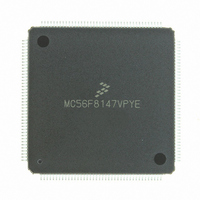
MC56F8147VPYE Freescale Semiconductor, MC56F8147VPYE Datasheet - Page 20

MC56F8147VPYE
Manufacturer Part Number
MC56F8147VPYE
Description
IC DSP 16BIT 40MHZ 160-LQFP
Manufacturer
Freescale Semiconductor
Series
56F8xxxr
Datasheet
1.MC56F8147VPYE.pdf
(172 pages)
Specifications of MC56F8147VPYE
Core Processor
56800
Core Size
16-Bit
Speed
40MHz
Connectivity
EBI/EMI, SCI, SPI
Peripherals
POR, PWM, WDT
Number Of I /o
76
Program Memory Size
128KB (64K x 16)
Program Memory Type
FLASH
Ram Size
4K x 16
Voltage - Supply (vcc/vdd)
2.25 V ~ 3.6 V
Data Converters
A/D 16x12b
Oscillator Type
External
Operating Temperature
-40°C ~ 105°C
Package / Case
160-LQFP
Data Bus Width
16 bit
Processor Series
MC56F81xx
Core
56800E
Data Ram Size
4 KB
Interface Type
SPI, SCI, CAN
Maximum Clock Frequency
40 MHz
Number Of Programmable I/os
76
Number Of Timers
2
Maximum Operating Temperature
+ 105 C
Mounting Style
SMD/SMT
Minimum Operating Temperature
- 40 C
On-chip Adc
4 x 12 bit, 4 Channel
Lead Free Status / RoHS Status
Lead free / RoHS Compliant
Eeprom Size
-
Lead Free Status / Rohs Status
Lead free / RoHS Compliant
Available stocks
Company
Part Number
Manufacturer
Quantity
Price
Company:
Part Number:
MC56F8147VPYE
Manufacturer:
FREESCAL
Quantity:
253
Company:
Part Number:
MC56F8147VPYE
Manufacturer:
Freescale Semiconductor
Quantity:
10 000
20
Table 2-2 Signal and Package Information for the 160-Pin LQFP and MBGA (Continued)
Signal Name
(GPIOA10)
(GPIOA11)
(GPIOA12)
(GPIOA13)
(GPIOA8)
(GPIOA9)
CLKO
XTAL
A0
A1
A2
A3
A4
A5
154
Pin
No.
93
10
11
12
13
14
3
Ball
K12
No.
D3
C3
E3
E4
F2
F1
F3
Output
Output
Output
Output
Input/
Input/
Type
56F8347 Technical Data, Rev.11
disabled,
pull-up is
output is
disabled
output is
In reset,
In reset,
enabled
During
Reset
driven
State
Chip-
Crystal Oscillator Output — This output connects the
internal crystal oscillator output to an external crystal.
If an external clock is used, XTAL must be used as the input
and EXTAL connected to GND.
The input clock can be selected to provide the clock directly
to the core. This input clock can also be selected as the input
clock for the on-chip PLL.
Clock Output — This pin outputs a buffered clock signal.
Using the SIM CLKO Select Register (SIM_CLKOSR), this
pin can be programmed as any of the following: disabled,
CLK_MSTR (system clock), IPBus clock, oscillator output,
prescaler clock and postscaler clock. Other signals are also
available for test purposes.
See
Address Bus — A0 - A5 specify six of the address lines for
external program or data memory accesses.
Depending upon the state of the DRV bit in the EMI bus
control register (BCR), A0 - A5 and EMI control signals are
tri-stated when the external bus is inactive.
Most designs will want to change the DRV state to DRV = 1
instead of using the default setting.
Port A GPIO — These six GPIO pins can be individually
programmed as input or output pins.
After reset, the default state is Address Bus.
To deactivate the internal pull-up resistor, clear the
appropriate GPIO bit in the GPIOA_PUR register.
Example: GPIOA8, clear bit 8 in the GPIOA_PUR register.
Part 6.5.7
for details.
Signal Description
Freescale Semiconductor
Preliminary


