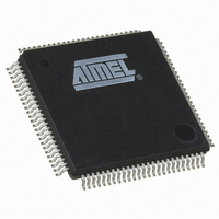
ATSAM3S4CA-AU Atmel, ATSAM3S4CA-AU Datasheet - Page 372

ATSAM3S4CA-AU
Manufacturer Part Number
ATSAM3S4CA-AU
Description
IC MCU 32BIT 256KB FLASH 100LQFP
Manufacturer
Atmel
Series
SAM3Sr
Specifications of ATSAM3S4CA-AU
Core Processor
ARM® Cortex-M3™
Core Size
32-Bit
Speed
64MHz
Connectivity
EBI/EMI, I²C, MMC, SPI, SSC, UART/USART, USB
Peripherals
Brown-out Detect/Reset, DMA, I²S, POR, PWM, WDT
Number Of I /o
79
Program Memory Size
256KB (256K x 8)
Program Memory Type
FLASH
Ram Size
48K x 8
Voltage - Supply (vcc/vdd)
1.62 V ~ 1.95 V
Data Converters
A/D 16x10/12b, D/A 2x12b
Oscillator Type
Internal
Operating Temperature
-40°C ~ 85°C
Package / Case
100-LQFP
Controller Family/series
ATSAM3S
No. Of I/o's
79
Ram Memory Size
48KB
Cpu Speed
64MHz
No. Of Timers
6
Rohs Compliant
Yes
Processor Series
ATSAM3x
Core
ARM Cortex M3
3rd Party Development Tools
JTRACE-CM3, MDK-ARM, RL-ARM, ULINK2
Development Tools By Supplier
ATSAM3S-EK
Cpu Family
AT91
Device Core
ARM Cortex-M3
Device Core Size
32b
Frequency (max)
64MHz
Total Internal Ram Size
48KB
# I/os (max)
79
Number Of Timers - General Purpose
6
Operating Supply Voltage (typ)
1.8/3.3V
Operating Supply Voltage (max)
1.95/3.6V
Operating Supply Voltage (min)
1.62V
On-chip Adc
16-chx12-bit
On-chip Dac
2-chx12-bit
Instruction Set Architecture
RISC
Operating Temp Range
-40C to 85C
Operating Temperature Classification
Industrial
Mounting
Surface Mount
Pin Count
100
Package Type
LQFP
Lead Free Status / RoHS Status
Lead free / RoHS Compliant
Eeprom Size
-
Lead Free Status / Rohs Status
Details
Available stocks
Company
Part Number
Manufacturer
Quantity
Price
Part Number:
ATSAM3S4CA-AU
Manufacturer:
ATMEL/爱特梅尔
Quantity:
20 000
- Current page: 372 of 1118
- Download datasheet (24Mb)
23.8.3
23.8.3.1
23.8.3.2
372
SAM3S Preliminary
Write Waveforms
NWE Waveforms
NCS Waveforms
The write protocol is similar to the read protocol. It is depicted in
starts with the address setting on the memory address bus.
The NWE signal is characterized by a setup timing, a pulse width and a hold timing.
The NCS signal waveforms in write operation are not the same that those applied in read opera-
tions, but are separately defined:
Figure 23-9. Write Cycle
1. NWE_SETUP: the NWE setup time is defined as the setup of address and data before
2. NWE_PULSE: The NWE pulse length is the time between NWE falling edge and NWE
3. NWE_HOLD: The NWE hold time is defined as the hold time of address and data after
1. NCS_WR_SETUP: the NCS setup time is defined as the setup time of address before
2. NCS_WR_PULSE: the NCS pulse length is the time between NCS falling edge and
3. NCS_WR_HOLD: the NCS hold time is defined as the hold time of address after the
the NWE falling edge;
rising edge;
the NWE rising edge.
the NCS falling edge.
NCS rising edge;
NCS rising edge.
A [23:0]
NWE
MCK
NCS
NCS_WR_SETUP
NWE_SETUP
NCS_WR_PULSE
NWE_PULSE
NWE_CYCLE
NWE_HOLD
Figure
NCS_WR_HOLD
23-9. The write cycle
6500C–ATARM–8-Feb-11
Related parts for ATSAM3S4CA-AU
Image
Part Number
Description
Manufacturer
Datasheet
Request
R

Part Number:
Description:
KIT EVAL FOR ATSAM3S4C
Manufacturer:
Atmel
Datasheet:

Part Number:
Description:
Development Boards & Kits - ARM EVAL KIT SAM3S8 & SAM3SD8 series
Manufacturer:
Atmel
Datasheet:

Part Number:
Description:
AT91 ARM Cortex M3-based Processor
Manufacturer:
ATMEL [ATMEL Corporation]
Datasheet:

Part Number:
Description:
DEV KIT FOR AVR/AVR32
Manufacturer:
Atmel
Datasheet:

Part Number:
Description:
INTERVAL AND WIPE/WASH WIPER CONTROL IC WITH DELAY
Manufacturer:
ATMEL Corporation
Datasheet:

Part Number:
Description:
Low-Voltage Voice-Switched IC for Hands-Free Operation
Manufacturer:
ATMEL Corporation
Datasheet:

Part Number:
Description:
MONOLITHIC INTEGRATED FEATUREPHONE CIRCUIT
Manufacturer:
ATMEL Corporation
Datasheet:

Part Number:
Description:
AM-FM Receiver IC U4255BM-M
Manufacturer:
ATMEL Corporation
Datasheet:

Part Number:
Description:
Monolithic Integrated Feature Phone Circuit
Manufacturer:
ATMEL Corporation
Datasheet:

Part Number:
Description:
Multistandard Video-IF and Quasi Parallel Sound Processing
Manufacturer:
ATMEL Corporation
Datasheet:

Part Number:
Description:
High-performance EE PLD
Manufacturer:
ATMEL Corporation
Datasheet:

Part Number:
Description:
8-bit Flash Microcontroller
Manufacturer:
ATMEL Corporation
Datasheet:


