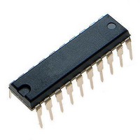
MCHC705JJ7CPE Freescale Semiconductor, MCHC705JJ7CPE Datasheet - Page 120

MCHC705JJ7CPE
Manufacturer Part Number
MCHC705JJ7CPE
Description
IC MCU 8BIT 224 BYTES RAM 20PDIP
Manufacturer
Freescale Semiconductor
Series
HC05r
Datasheet
1.MC705JJ7CDWE.pdf
(164 pages)
Specifications of MCHC705JJ7CPE
Core Processor
HC05
Core Size
8-Bit
Speed
2.1MHz
Connectivity
SIO
Peripherals
POR, Temp Sensor, WDT
Number Of I /o
14
Program Memory Size
6KB (6K x 8)
Program Memory Type
OTP
Ram Size
224 x 8
Voltage - Supply (vcc/vdd)
2.7 V ~ 5.5 V
Data Converters
A/D 4x12b
Oscillator Type
Internal
Operating Temperature
-40°C ~ 85°C
Package / Case
20-DIP (0.300", 7.62mm)
Processor Series
HC705JJ
Core
HC05
Data Bus Width
8 bit
Data Ram Size
224 B
Interface Type
SIOP
Maximum Clock Frequency
2.1 MHz
Number Of Programmable I/os
14
Number Of Timers
2
Maximum Operating Temperature
+ 85 C
Mounting Style
Through Hole
Minimum Operating Temperature
- 40 C
On-chip Adc
12 bit, 4 Channel
Package
20PDIP
Family Name
HC05
Maximum Speed
2.1 MHz
Operating Supply Voltage
3.3|5 V
Lead Free Status / RoHS Status
Lead free / RoHS Compliant
Eeprom Size
-
Lead Free Status / Rohs Status
Details
EPROM/OTPROM
ELAT — EPROM Bus Latch Bit
Whenever the ELAT bit is cleared, the EPGM bit is also cleared. Both the EPGM and the ELAT bit cannot
be set using the same write instruction. Any attempt to set both the ELAT and EPGM bit on the same write
instruction cycle will result in the ELAT bit being set and the EPGM bit being cleared. To program a byte
of EPROM, manipulate the EPROG register as follows:
13.2.2 Mask Option Register
The mask option register (MOR) shown in
The MOR is unaffected by reset. The erased state of the MOR is $00. The options that can be
programmed by the MOR are:
SWPDI — Software Pulldown Inhibit Bit
120
1. Set the ELAT bit in the EPROG register.
2. Write the desired data to the desired EPROM address.
3. Set the EPGM bit in the EPROG register for the specified programming time, t
4. Clear the ELAT and EPGM bits in the EPROG register.
1. Port software programmable pulldown devices (enable or disable)
2. Startup delay after stop (16 or 4064 cycles)
3. Oscillator shunt resistor (2 MΩ or open)
4. STOP instruction (enable or disable)
5. Low-voltage reset (enable or disable)
6. Port A external interrupt function (enable or disable)
7. IRQ trigger sensitivity (edge-triggered only or both edge- and level-triggered)
8. COP watchdog (enable or disable)
This read/write bit configures address and data buses for programming the EPROM array. EPROM
data cannot be read when ELAT is set. Clearing the ELAT bit also clears the EPGM bit. Reset clears
ELAT.
This EPROM bit inhibits software control of the port A and port B pulldown devices.
1 = Address and data buses configured for EPROM programming of the array. The address and
0 = Address and data buses configured for normal operation
1 = Software pulldown inhibited
0 = Software pulldown enabled
data buses are latched in the EPROM array when a subsequent write to the array is made. Data
in the EPROM array cannot be read.
Address:
Erased:
Reset:
Read:
Write:
MC68HC705JJ7 • MC68HC705JP7 Advance Information Data Sheet, Rev. 4.1
SWPDI
$1FF1
Bit 7
0
Figure 13-2. Mask Option Register (MOR)
DELAY
6
0
OSCRES
Figure 13-2
5
0
Unaffected by reset
SWAIT
4
0
is an EPROM byte that controls eight mask options.
LVREN
3
0
PIRQ
2
0
LEVEL
1
0
Freescale Semiconductor
EPGM
COPEN
Bit 0
0
.


