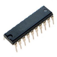
MCHC705JJ7CPE Freescale Semiconductor, MCHC705JJ7CPE Datasheet - Page 31

MCHC705JJ7CPE
Manufacturer Part Number
MCHC705JJ7CPE
Description
IC MCU 8BIT 224 BYTES RAM 20PDIP
Manufacturer
Freescale Semiconductor
Series
HC05r
Datasheet
1.MC705JJ7CDWE.pdf
(164 pages)
Specifications of MCHC705JJ7CPE
Core Processor
HC05
Core Size
8-Bit
Speed
2.1MHz
Connectivity
SIO
Peripherals
POR, Temp Sensor, WDT
Number Of I /o
14
Program Memory Size
6KB (6K x 8)
Program Memory Type
OTP
Ram Size
224 x 8
Voltage - Supply (vcc/vdd)
2.7 V ~ 5.5 V
Data Converters
A/D 4x12b
Oscillator Type
Internal
Operating Temperature
-40°C ~ 85°C
Package / Case
20-DIP (0.300", 7.62mm)
Processor Series
HC705JJ
Core
HC05
Data Bus Width
8 bit
Data Ram Size
224 B
Interface Type
SIOP
Maximum Clock Frequency
2.1 MHz
Number Of Programmable I/os
14
Number Of Timers
2
Maximum Operating Temperature
+ 85 C
Mounting Style
Through Hole
Minimum Operating Temperature
- 40 C
On-chip Adc
12 bit, 4 Channel
Package
20PDIP
Family Name
HC05
Maximum Speed
2.1 MHz
Operating Supply Voltage
3.3|5 V
Lead Free Status / RoHS Status
Lead free / RoHS Compliant
Eeprom Size
-
Lead Free Status / Rohs Status
Details
3.6 Condition Code Register
The condition code register is an 8-bit register whose three most significant bits are permanently fixed at
111 as shown in
indicate the results of the instruction just executed. The following paragraphs describe the functions of the
condition code register.
Half-Carry Flag (H)
Interrupt Mask (I)
Negative Flag (N)
Zero Flag (Z)
Carry/Borrow Flag (C)
3.7 Arithmetic/Logic Unit (ALU)
The ALU performs the arithmetic and logical operations defined by the instruction set. The binary
arithmetic circuits decode instructions and set up the ALU for the selected operation. Most binary
arithmetic is based on the addition algorithm, carrying out subtraction as negative addition. Multiplication
is not performed as a discrete operation but as a chain of addition and shift operations within the ALU.
The multiply instruction (MUL) requires 11 internal clock cycles to complete this chain of operations.
Freescale Semiconductor
The CPU sets the half-carry flag when a carry occurs between bits 3 and 4 of the accumulator during
an ADD or ADC operation. The half-carry flag is required for binary coded decimal (BCD) arithmetic
operations. Reset has no effect on the half-carry flag.
Setting the interrupt mask disables interrupts. If an interrupt request occurs while the interrupt mask is
a logic 0, the CPU saves the CPU registers on the stack, sets the interrupt mask, and then fetches the
interrupt vector. If an interrupt request occurs while the interrupt mask is set, the interrupt request is
latched. The CPU processes the latched interrupt as soon as the interrupt mask is cleared again.
A return-from-interrupt (RTI) instruction pulls the CPU registers from the stack, restoring the interrupt
mask to its cleared state. After a reset, the interrupt mask is set and can be cleared only by a CLI
instruction.
The CPU sets the negative flag when an arithmetic operation, logical operation, or data manipulation
produces a negative result. Reset has no affect on the negative flag.
The CPU sets the zero flag when an arithmetic operation, logical operation, or data manipulation
produces a result of $00. Reset has no affect on the zero flag.
The CPU sets the carry/borrow flag when an addition operation produces a carry out of bit 7 of the
accumulator or when a subtraction operation requires a borrow. Some logical operations and data
manipulation instructions also clear or set the carry/borrow flag. Reset has no effect on the
carry/borrow flag.
Reset:
Read:
Write:
Figure
MC68HC705JJ7 • MC68HC705JP7 Advance Information Data Sheet, Rev. 4.1
Bit 7
U = Unaffected
3-6. The condition code register contains the interrupt mask and four flags that
1
1
Figure 3-6. Condition Code Register (CCR)
6
1
1
5
1
1
H
U
4
3
1
I
N
U
2
C
U
1
Condition Code Register
Bit 0
U
Z
31


