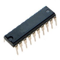
MCHC705JJ7CPE Freescale Semiconductor, MCHC705JJ7CPE Datasheet - Page 57

MCHC705JJ7CPE
Manufacturer Part Number
MCHC705JJ7CPE
Description
IC MCU 8BIT 224 BYTES RAM 20PDIP
Manufacturer
Freescale Semiconductor
Series
HC05r
Datasheet
1.MC705JJ7CDWE.pdf
(164 pages)
Specifications of MCHC705JJ7CPE
Core Processor
HC05
Core Size
8-Bit
Speed
2.1MHz
Connectivity
SIO
Peripherals
POR, Temp Sensor, WDT
Number Of I /o
14
Program Memory Size
6KB (6K x 8)
Program Memory Type
OTP
Ram Size
224 x 8
Voltage - Supply (vcc/vdd)
2.7 V ~ 5.5 V
Data Converters
A/D 4x12b
Oscillator Type
Internal
Operating Temperature
-40°C ~ 85°C
Package / Case
20-DIP (0.300", 7.62mm)
Processor Series
HC705JJ
Core
HC05
Data Bus Width
8 bit
Data Ram Size
224 B
Interface Type
SIOP
Maximum Clock Frequency
2.1 MHz
Number Of Programmable I/os
14
Number Of Timers
2
Maximum Operating Temperature
+ 85 C
Mounting Style
Through Hole
Minimum Operating Temperature
- 40 C
On-chip Adc
12 bit, 4 Channel
Package
20PDIP
Family Name
HC05
Maximum Speed
2.1 MHz
Operating Supply Voltage
3.3|5 V
Lead Free Status / RoHS Status
Lead free / RoHS Compliant
Eeprom Size
-
Lead Free Status / Rohs Status
Details
PDICL — Lower Port C Pulldown Inhibit Bits (MC68HC705JP7)
PDIA5–PDIA0 — Port A Pulldown Inhibit Bits
7.2.4 Port A External Interrupts
The PIRQ bit in the MOR enables the PA3–PA0 pins to serve as external interrupt pins in addition to the
IRQ/V
PIRQ bit in the MOR determines whether external interrupt inputs are edge-sensitive only or both edge-
and level-sensitive. Port A interrupts are also interactive with each other and the IRQ/V
in
7.2.5 Port A Logic
When a PA0:PA5 pin is programmed as an output, reading the port bit actually reads the value of the data
latch and not the voltage on the pin itself. When a PA0:PA5 pin is programmed as an input, reading the
port bit reads the voltage level on the pin. The data latch can always be written, regardless of the state of
its DDR bit.
The data latch can always be written, regardless of the state of its DDR bits.
operations of the port A pins.
Freescale Semiconductor
1. DDRA can always be read or written.
2. Don’t care
4.5 External
Writing to this write-only bit controls the port C pulldown devices on the lower four bits (PC0–PC3).
Reading these pulldown register A bits returns undefined data. Reset clears bit PDICL.
Writing to these write-only bits controls the port A pulldown devices. Reading these pulldown register
A bits returns undefined data. Reset clears bits PDIA5–PDIA0.
Port A
Pin(s)
PA0
PA1
PA2
PA3
PA4
PA5
1 = Lower four port C pins pulldown devices turned off
0 = Lower four port C pins pulldown devices turned on if pin has been programmed by the DDRC
1 = Corresponding port A pin pulldown device turned off
0 = Corresponding port A pin pulldown device turned on if pin has been programmed by the DDRA
PP
pin. The active interrupt state for the PA3–PA0 pins is a logic 1 or a rising edge. A state of the
to be an input
to be an input
Figure 7-4
When testing for external interrupts, the BIH and BIL instructions test the
voltage on the IRQ/V
Therefore, BIH and BIL cannot test the port A external interrupt pins.
Interrupts.
(in MOR)
SWPDI
X
MC68HC705JJ7 • MC68HC705JP7 Advance Information Data Sheet, Rev. 4.1
0
0
1
(2)
shows the I/O logic of PA0–PA5 pins of port A.
PDIAx
X
X
0
1
(2)
Table 7-1. Port A Pin Functions
PP
Port A
pin, not the state of the internal IRQ signal.
DDRAx
0
0
0
1
(1)
NOTE
(Pin or Data Register)
Read
Data
Pin
Pin
Pin
PORTA Access
Write
Data
Data
Data
Data
Table 7-1
Pulldown
On
Off
Off
Off
PP
Port A Pins
Result on
summarizes the
pin as described
PAx out
PAx in
PAx in
PAx in
Pin
Port A
57


