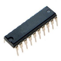
MCHC705JJ7CPE Freescale Semiconductor, MCHC705JJ7CPE Datasheet - Page 60

MCHC705JJ7CPE
Manufacturer Part Number
MCHC705JJ7CPE
Description
IC MCU 8BIT 224 BYTES RAM 20PDIP
Manufacturer
Freescale Semiconductor
Series
HC05r
Datasheet
1.MC705JJ7CDWE.pdf
(164 pages)
Specifications of MCHC705JJ7CPE
Core Processor
HC05
Core Size
8-Bit
Speed
2.1MHz
Connectivity
SIO
Peripherals
POR, Temp Sensor, WDT
Number Of I /o
14
Program Memory Size
6KB (6K x 8)
Program Memory Type
OTP
Ram Size
224 x 8
Voltage - Supply (vcc/vdd)
2.7 V ~ 5.5 V
Data Converters
A/D 4x12b
Oscillator Type
Internal
Operating Temperature
-40°C ~ 85°C
Package / Case
20-DIP (0.300", 7.62mm)
Processor Series
HC705JJ
Core
HC05
Data Bus Width
8 bit
Data Ram Size
224 B
Interface Type
SIOP
Maximum Clock Frequency
2.1 MHz
Number Of Programmable I/os
14
Number Of Timers
2
Maximum Operating Temperature
+ 85 C
Mounting Style
Through Hole
Minimum Operating Temperature
- 40 C
On-chip Adc
12 bit, 4 Channel
Package
20PDIP
Family Name
HC05
Maximum Speed
2.1 MHz
Operating Supply Voltage
3.3|5 V
Lead Free Status / RoHS Status
Lead free / RoHS Compliant
Eeprom Size
-
Lead Free Status / Rohs Status
Details
Parallel Input/Output
7.3.4 Port B Logic
All port B pins have the general I/O port logic similar to port A; but they also share this function with inputs
or outputs from other modules, which are also attached to the pin itself or override the general I/O
function. PB0, PB1, PB2, and PB3 simply share their inputs with another module. PB4, PB5, PB6, and
PB7 will have their operation altered by outputs or controls from other modules.
7.3.5 PB0, PBI, PB2, and PB3 Logic
The typical I/O logic shown in
port B pins are programmed as an output, reading the port bit actually reads the value of the data latch
and not the voltage on the pin itself. When these port B pins are programmed as an input, reading the port
bit reads the voltage level on the pin. The data latch can always be written, regardless of the state of its
DDRB bit. The operations of the PB0–PB3 pins are summarized in
The PB0–PB3 pins share their inputs with another module. When using the other attached module, these
conditions must be observed:
60
1. If the DDRB configures the pin as an output, then the port data register can provide an output which
2. If the DDRB configures the pin as an input, then reading the port data register will return the state
3. If DDRB configures the pin as an input and the pulldown device is activated for a pin, it will also
4. If interaction between the port logic and the other module is not desired, the pin should be
may conflict with any external input source to the other module. The pulldown device will be
disabled in this case.
of the input in terms of the digital threshold for that pin (analog inputs will default to logic states).
load the input to the other module.
configured as an input by clearing the appropriate DDRB bit. The input pulldown device is disabled
by clearing the appropriate PDRB bit (or by disabling programmable pulldowns with the SWPDI bit
in the MOR).
WRITE $0001
WRITE $0005
READ $0005
READ $0001
WRITE $0011
RESET
MC68HC705JJ7 • MC68HC705JP7 Advance Information Data Sheet, Rev. 4.1
Figure 7-8
R
R
PORT BDATA
Figure 7-8. PB0–PB3 Pin I/O Circuit
DATA DIRECTION
REGISTER
BIT PBx
REGISTER B
PULLDOWN
REGISTER B
BIT DDRBx
BIT PDIBx
is used for PB0, PB1, PB2, and PB3 pins of port B. When these
MASK OPTION REG. ($1FF1)
Table
7-2.
(PINS PB0, PB1, PB2, PB3)
TIMER INPUT CAPTURE
AND PROGRAMMABLE
ANALOG SUBSYSTEM,
Freescale Semiconductor
PULLDOWN
DEVICE
PBx


