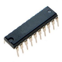
MCHC705JJ7CPE Freescale Semiconductor, MCHC705JJ7CPE Datasheet - Page 73

MCHC705JJ7CPE
Manufacturer Part Number
MCHC705JJ7CPE
Description
IC MCU 8BIT 224 BYTES RAM 20PDIP
Manufacturer
Freescale Semiconductor
Series
HC05r
Datasheet
1.MC705JJ7CDWE.pdf
(164 pages)
Specifications of MCHC705JJ7CPE
Core Processor
HC05
Core Size
8-Bit
Speed
2.1MHz
Connectivity
SIO
Peripherals
POR, Temp Sensor, WDT
Number Of I /o
14
Program Memory Size
6KB (6K x 8)
Program Memory Type
OTP
Ram Size
224 x 8
Voltage - Supply (vcc/vdd)
2.7 V ~ 5.5 V
Data Converters
A/D 4x12b
Oscillator Type
Internal
Operating Temperature
-40°C ~ 85°C
Package / Case
20-DIP (0.300", 7.62mm)
Processor Series
HC705JJ
Core
HC05
Data Bus Width
8 bit
Data Ram Size
224 B
Interface Type
SIOP
Maximum Clock Frequency
2.1 MHz
Number Of Programmable I/os
14
Number Of Timers
2
Maximum Operating Temperature
+ 85 C
Mounting Style
Through Hole
Minimum Operating Temperature
- 40 C
On-chip Adc
12 bit, 4 Channel
Package
20PDIP
Family Name
HC05
Maximum Speed
2.1 MHz
Operating Supply Voltage
3.3|5 V
Lead Free Status / RoHS Status
Lead free / RoHS Compliant
Eeprom Size
-
Lead Free Status / Rohs Status
Details
- Current page: 73 of 164
- Download datasheet (2Mb)
8.2 Analog Multiplex Register
The analog multiplex register (AMUX) controls the general interconnection and operation. The control bits
in the AMUX are shown in
HOLD, DHOLD
Freescale Semiconductor
These read/write bits control the source connection to the negative input of voltage comparator 2
shown in
selection bus, or the divide-by-two channel selection bus to charge the internal sample capacitor and
to also be presented to comparator 2. The decoding of these sources is given in
During the hold case when both the HOLD and DHOLD bits are clear, the VOFF bit in the analog status
register (ASR) can offset the V
offset source is bypassed whenever the sample capacitor is being charged with either the HOLD or
DHOLD bit set. The VOFF bit must be enabled by the OPT bit in the COPR at location $1FF0.
Figure
Address:
TEMPERATURE
Reset:
Read:
Write:
INTERNAL
DIODE
SELECTION
CHANNEL
MC68HC705JJ7 • MC68HC705JP7 Advance Information Data Sheet, Rev. 4.1
8-3. This allows the voltage on the internal temperature sensing diode, the channel
BUS
$0003
HOLD
Bit 7
1
V
DD
Figure
Figure 8-2. Analog Multiplex Register (AMUX)
Figure 8-3. Comparator 2 Input Circuit
DHOLD
OFFSET
V
SS
8-2.
6
0
SS
80 kΩ
80 kΩ
reference on the sample capacitor by approximately 100 mV. This
INV
5
0
PB0
SAMPLE
CAP
+
–
VREF
COMP2
4
0
MUX4
3
0
MUX3
2
0
MUX2
1
0
Analog Multiplex Register
V
OPT (MOR)
HOLD
DHOLD
OFF
Table
MUX1
Bit 0
0
8-1.
73
Related parts for MCHC705JJ7CPE
Image
Part Number
Description
Manufacturer
Datasheet
Request
R
Part Number:
Description:
Manufacturer:
Freescale Semiconductor, Inc
Datasheet:
Part Number:
Description:
Manufacturer:
Freescale Semiconductor, Inc
Datasheet:
Part Number:
Description:
Manufacturer:
Freescale Semiconductor, Inc
Datasheet:
Part Number:
Description:
Manufacturer:
Freescale Semiconductor, Inc
Datasheet:
Part Number:
Description:
Manufacturer:
Freescale Semiconductor, Inc
Datasheet:
Part Number:
Description:
Manufacturer:
Freescale Semiconductor, Inc
Datasheet:
Part Number:
Description:
Manufacturer:
Freescale Semiconductor, Inc
Datasheet:
Part Number:
Description:
Manufacturer:
Freescale Semiconductor, Inc
Datasheet:
Part Number:
Description:
Manufacturer:
Freescale Semiconductor, Inc
Datasheet:
Part Number:
Description:
Manufacturer:
Freescale Semiconductor, Inc
Datasheet:
Part Number:
Description:
Manufacturer:
Freescale Semiconductor, Inc
Datasheet:
Part Number:
Description:
Manufacturer:
Freescale Semiconductor, Inc
Datasheet:
Part Number:
Description:
Manufacturer:
Freescale Semiconductor, Inc
Datasheet:
Part Number:
Description:
Manufacturer:
Freescale Semiconductor, Inc
Datasheet:
Part Number:
Description:
Manufacturer:
Freescale Semiconductor, Inc
Datasheet:


