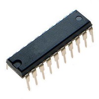
MCHC705JJ7CPE Freescale Semiconductor, MCHC705JJ7CPE Datasheet - Page 93

MCHC705JJ7CPE
Manufacturer Part Number
MCHC705JJ7CPE
Description
IC MCU 8BIT 224 BYTES RAM 20PDIP
Manufacturer
Freescale Semiconductor
Series
HC05r
Datasheet
1.MC705JJ7CDWE.pdf
(164 pages)
Specifications of MCHC705JJ7CPE
Core Processor
HC05
Core Size
8-Bit
Speed
2.1MHz
Connectivity
SIO
Peripherals
POR, Temp Sensor, WDT
Number Of I /o
14
Program Memory Size
6KB (6K x 8)
Program Memory Type
OTP
Ram Size
224 x 8
Voltage - Supply (vcc/vdd)
2.7 V ~ 5.5 V
Data Converters
A/D 4x12b
Oscillator Type
Internal
Operating Temperature
-40°C ~ 85°C
Package / Case
20-DIP (0.300", 7.62mm)
Processor Series
HC705JJ
Core
HC05
Data Bus Width
8 bit
Data Ram Size
224 B
Interface Type
SIOP
Maximum Clock Frequency
2.1 MHz
Number Of Programmable I/os
14
Number Of Timers
2
Maximum Operating Temperature
+ 85 C
Mounting Style
Through Hole
Minimum Operating Temperature
- 40 C
On-chip Adc
12 bit, 4 Channel
Package
20PDIP
Family Name
HC05
Maximum Speed
2.1 MHz
Operating Supply Voltage
3.3|5 V
Lead Free Status / RoHS Status
Lead free / RoHS Compliant
Eeprom Size
-
Lead Free Status / Rohs Status
Details
8.7.2 Voltage Comparator 2
Voltage comparator 2 can be used as a simple comparator if its charge current source and discharge
device are disabled by clearing the ISEN bit in the ACR. If the ISEN bit is set, the internal ramp discharge
device connected to PB0/AN0 may become active and try to pull down any voltage source that may be
connected to that pin. Also, since voltage comparator 2 is always connected to two of the port B I/O pins,
these pins should be configured as inputs and have their software programmable pulldowns disabled.
8.8 Current Source Features
The internal current source connected to the PB0/AN0 pin supplies about 100 µA of current when the
discharge device is disabled and the current source is active. Therefore, this current source can be used
in an application if the ISEN enable bit is set to power up the current source and by setting the A/D
conversion method to manual mode 0 (ATD1 and ATD2 cleared) and the charge current enabled (CHG
set).
8.9 Internal Temperature Sensing Diode Features
An internal diode is forward biased to V
centigrade rise in the temperature of the device. This temperature sensing diode is powered up from a
current source only during the time that the diode is selected. When on, this current source typically adds
about 30 µA to the I
The temperature sensing diode can be selected by setting both the HOLD and DHOLD bits in the AMUX
register (see
8.10 Sample and Hold
When using the internal sample capacitor to capture a voltage for later conversion, the HOLD or DHOLD
bit must be cleared first before changing any channel selection. If both the HOLD (or DHOLD) bit and the
channel selection are changed on the same write cycle, the sample may be corrupted during the switching
transitions.
The additional option of adding an offset voltage to the bottom of the sample capacitor allows unknown
voltages near V
caused by a single V
regardless of the comparator offset to determine N
Methods. In either case the OPT bit must be set in the COPR located at $1FF0 as in
VOFF bit must be set in the ASR. It is not necessary to switch the VOFF bit during conversions, since the
offset is controlled by the HOLD and DHOLD bits when the VOFF is active. Refer to
Register
Freescale Semiconductor
for more details on the design and decoding of the sample and hold circuit.
8.2 Analog Multiplex
The sample capacitor can be affected by excessive noise created with
respect to the device’s V
charge up depending on the voltage level stored on the sample capacitor.
It is recommended to avoid switching large currents through the port pins
while a voltage is to remain stored on the sample capacitor.
SS
to be sampled and then shifted up past the comparator offset and the device offset
MC68HC705JJ7 • MC68HC705JP7 Advance Information Data Sheet, Rev. 4.1
DD
SS
current.
return pin. This offset also provides a means to measure the internal V
Register).
SS
SS
and will have its voltage change, V
pin such that it may appear to leak down or
NOTE
OFF
as described in
8.6 Voltage Measurement
D
, for each degree
Current Source Features
8.2 Analog Multiplex
Figure 8-12
SS
and the
level
93


