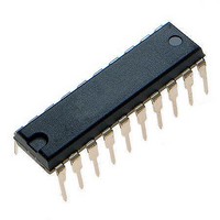
MCHC705JJ7CPE Freescale Semiconductor, MCHC705JJ7CPE Datasheet - Page 75

MCHC705JJ7CPE
Manufacturer Part Number
MCHC705JJ7CPE
Description
IC MCU 8BIT 224 BYTES RAM 20PDIP
Manufacturer
Freescale Semiconductor
Series
HC05r
Datasheet
1.MC705JJ7CDWE.pdf
(164 pages)
Specifications of MCHC705JJ7CPE
Core Processor
HC05
Core Size
8-Bit
Speed
2.1MHz
Connectivity
SIO
Peripherals
POR, Temp Sensor, WDT
Number Of I /o
14
Program Memory Size
6KB (6K x 8)
Program Memory Type
OTP
Ram Size
224 x 8
Voltage - Supply (vcc/vdd)
2.7 V ~ 5.5 V
Data Converters
A/D 4x12b
Oscillator Type
Internal
Operating Temperature
-40°C ~ 85°C
Package / Case
20-DIP (0.300", 7.62mm)
Processor Series
HC705JJ
Core
HC05
Data Bus Width
8 bit
Data Ram Size
224 B
Interface Type
SIOP
Maximum Clock Frequency
2.1 MHz
Number Of Programmable I/os
14
Number Of Timers
2
Maximum Operating Temperature
+ 85 C
Mounting Style
Through Hole
Minimum Operating Temperature
- 40 C
On-chip Adc
12 bit, 4 Channel
Package
20PDIP
Family Name
HC05
Maximum Speed
2.1 MHz
Operating Supply Voltage
3.3|5 V
Lead Free Status / RoHS Status
Lead free / RoHS Compliant
Eeprom Size
-
Lead Free Status / Rohs Status
Details
- Current page: 75 of 164
- Download datasheet (2Mb)
VREF
MUX1:4
Freescale Semiconductor
V–
V+
This read/write bit connects the channel select bus to V
measurement. It cannot be selected if any of the other input sources to the channel select bus are
selected as shown in
These are read/write bits that connect the analog subsystem pins to the channel select bus and voltage
comparator 2 for purposes of making a voltage measurement. They can be selected individually or
combined with any of the other input sources to the channel select bus as shown in
1 = Channel select bus connected to V
0 = Channel select bus cannot be connected to V
Either comparator may generate an output flag when the inputs are
exchanged due to a change in the state of the INV bit. It is therefore
recommended that the INV bit not be changed while waiting for a
comparator flag. Further, any changes to the state of the INV bit should be
followed by writing a logic 1 to both the CPFR1 and CPFR2 bits to clear any
extraneous CPF1 or CPF2 flags that may have occurred.
The V
voltage generated by the total chip current passing through the package
bond wires and lead frame that are attached to the single V
offset raises the internal V
with respect to the external V
select bus connects it to this internal AV
When making A/D conversions, this AV
ramping capacitor since the discharge device on the PB0/AN0 pin
discharges the external capacitor to the internal AV
circumstances, the positive input (+) to comparator 2 will always be higher
than the negative input (–) until the negative input reaches the AV
voltage plus any offset in comparator 2.
MC68HC705JJ7 • MC68HC705JP7 Advance Information Data Sheet, Rev. 4.1
AOFF
V
Table
IO
voltage source shown in
+
–
COMP
8-2. This bit is cleared by a reset of the device.
INV = 0
RISE
WHEN
V+ > V–
Figure 8-4. INV Bit Action
SS
SS
reference (AV
DD
pin. Turning on the V
if all MUX1:4 are cleared.
NOTE
NOTE
Figure 8-1
SS
SS
DD
offset gets placed on the external
V+
V–
.
reference line.
SS
DD
) in the analog subsystem
for making a reference voltage
depicts a small offset
SS
SS
line. Under these
MUX to the channel
SS
pin. This
V
SS
IO
Analog Multiplex Register
offset
+
–
COMP
Table
INV = 1
8-2.
RISE
WHEN
V+ > V–
75
Related parts for MCHC705JJ7CPE
Image
Part Number
Description
Manufacturer
Datasheet
Request
R
Part Number:
Description:
Manufacturer:
Freescale Semiconductor, Inc
Datasheet:
Part Number:
Description:
Manufacturer:
Freescale Semiconductor, Inc
Datasheet:
Part Number:
Description:
Manufacturer:
Freescale Semiconductor, Inc
Datasheet:
Part Number:
Description:
Manufacturer:
Freescale Semiconductor, Inc
Datasheet:
Part Number:
Description:
Manufacturer:
Freescale Semiconductor, Inc
Datasheet:
Part Number:
Description:
Manufacturer:
Freescale Semiconductor, Inc
Datasheet:
Part Number:
Description:
Manufacturer:
Freescale Semiconductor, Inc
Datasheet:
Part Number:
Description:
Manufacturer:
Freescale Semiconductor, Inc
Datasheet:
Part Number:
Description:
Manufacturer:
Freescale Semiconductor, Inc
Datasheet:
Part Number:
Description:
Manufacturer:
Freescale Semiconductor, Inc
Datasheet:
Part Number:
Description:
Manufacturer:
Freescale Semiconductor, Inc
Datasheet:
Part Number:
Description:
Manufacturer:
Freescale Semiconductor, Inc
Datasheet:
Part Number:
Description:
Manufacturer:
Freescale Semiconductor, Inc
Datasheet:
Part Number:
Description:
Manufacturer:
Freescale Semiconductor, Inc
Datasheet:
Part Number:
Description:
Manufacturer:
Freescale Semiconductor, Inc
Datasheet:


