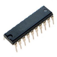
MCHC705JJ7CPE Freescale Semiconductor, MCHC705JJ7CPE Datasheet - Page 37

MCHC705JJ7CPE
Manufacturer Part Number
MCHC705JJ7CPE
Description
IC MCU 8BIT 224 BYTES RAM 20PDIP
Manufacturer
Freescale Semiconductor
Series
HC05r
Datasheet
1.MC705JJ7CDWE.pdf
(164 pages)
Specifications of MCHC705JJ7CPE
Core Processor
HC05
Core Size
8-Bit
Speed
2.1MHz
Connectivity
SIO
Peripherals
POR, Temp Sensor, WDT
Number Of I /o
14
Program Memory Size
6KB (6K x 8)
Program Memory Type
OTP
Ram Size
224 x 8
Voltage - Supply (vcc/vdd)
2.7 V ~ 5.5 V
Data Converters
A/D 4x12b
Oscillator Type
Internal
Operating Temperature
-40°C ~ 85°C
Package / Case
20-DIP (0.300", 7.62mm)
Processor Series
HC705JJ
Core
HC05
Data Bus Width
8 bit
Data Ram Size
224 B
Interface Type
SIOP
Maximum Clock Frequency
2.1 MHz
Number Of Programmable I/os
14
Number Of Timers
2
Maximum Operating Temperature
+ 85 C
Mounting Style
Through Hole
Minimum Operating Temperature
- 40 C
On-chip Adc
12 bit, 4 Channel
Package
20PDIP
Family Name
HC05
Maximum Speed
2.1 MHz
Operating Supply Voltage
3.3|5 V
Lead Free Status / RoHS Status
Lead free / RoHS Compliant
Eeprom Size
-
Lead Free Status / Rohs Status
Details
- Current page: 37 of 164
- Download datasheet (2Mb)
4.5.2 PA0–PA3 Pins
Programming the PIRQ bit in the MOR to a logic 1 enables the PA0–PA3 pins (PA0:3) to serve as
additional external interrupt sources. A rising edge on a PA0:3 pin latches an external interrupt request.
After completing the current instruction, the CPU tests the IRQ latch. If the IRQ latch is set, the CPU then
tests the I bit in the condition code register and the IRQE bit in the ISCR. If the I bit is clear and the IRQE
bit is set, the CPU then begins the interrupt sequence. The CPU clears the IRQ latch while it fetches the
interrupt vector, so that another external interrupt request can be latched during the interrupt service
routine. As soon as the I bit is cleared during the return from interrupt, the CPU can recognize the new
interrupt request.
The PA0:3 pins can be edge-triggered or edge- and level-triggered. External interrupt triggering sensitivity
is selected by the LEVEL bit in the MOR.
With the edge- and level-sensitive trigger MOR option, a rising edge or a high level on a PA0:3 pin latches
an external interrupt request. The edge- and level-sensitive trigger MOR option allows connection to a
PA0:3 pin of multiple wired-OR interrupt sources. As long as any source is holding the pin high, an
external interrupt request is present, and the CPU continues to execute the interrupt service routine.
Freescale Semiconductor
IRQ/V
PA0
PA3
PA2
PA1
MASK OPTION REGISTER ($1FF1)
PP
MC68HC705JJ7 • MC68HC705JP7 Advance Information Data Sheet, Rev. 4.1
Figure 4-3. External Interrupt Logic
IRQ VECTOR FETCH
INTERNAL DATA BUS
RST
V
DD
LATCH
IRQ
R
IRQ STATUS/CONTROL REGISTER ($000D)
External Interrupts
TO BIH & BIL
INSTRUCTION
PROCESSING
V
USER EPROM
AND PEPROM
EXTERNAL
INTERRUPT
REQUEST
PP
TO
37
Related parts for MCHC705JJ7CPE
Image
Part Number
Description
Manufacturer
Datasheet
Request
R
Part Number:
Description:
Manufacturer:
Freescale Semiconductor, Inc
Datasheet:
Part Number:
Description:
Manufacturer:
Freescale Semiconductor, Inc
Datasheet:
Part Number:
Description:
Manufacturer:
Freescale Semiconductor, Inc
Datasheet:
Part Number:
Description:
Manufacturer:
Freescale Semiconductor, Inc
Datasheet:
Part Number:
Description:
Manufacturer:
Freescale Semiconductor, Inc
Datasheet:
Part Number:
Description:
Manufacturer:
Freescale Semiconductor, Inc
Datasheet:
Part Number:
Description:
Manufacturer:
Freescale Semiconductor, Inc
Datasheet:
Part Number:
Description:
Manufacturer:
Freescale Semiconductor, Inc
Datasheet:
Part Number:
Description:
Manufacturer:
Freescale Semiconductor, Inc
Datasheet:
Part Number:
Description:
Manufacturer:
Freescale Semiconductor, Inc
Datasheet:
Part Number:
Description:
Manufacturer:
Freescale Semiconductor, Inc
Datasheet:
Part Number:
Description:
Manufacturer:
Freescale Semiconductor, Inc
Datasheet:
Part Number:
Description:
Manufacturer:
Freescale Semiconductor, Inc
Datasheet:
Part Number:
Description:
Manufacturer:
Freescale Semiconductor, Inc
Datasheet:
Part Number:
Description:
Manufacturer:
Freescale Semiconductor, Inc
Datasheet:


