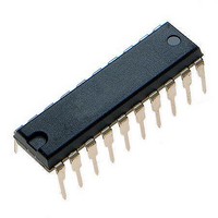
MCHC705JJ7CPE Freescale Semiconductor, MCHC705JJ7CPE Datasheet - Page 47

MCHC705JJ7CPE
Manufacturer Part Number
MCHC705JJ7CPE
Description
IC MCU 8BIT 224 BYTES RAM 20PDIP
Manufacturer
Freescale Semiconductor
Series
HC05r
Datasheet
1.MC705JJ7CDWE.pdf
(164 pages)
Specifications of MCHC705JJ7CPE
Core Processor
HC05
Core Size
8-Bit
Speed
2.1MHz
Connectivity
SIO
Peripherals
POR, Temp Sensor, WDT
Number Of I /o
14
Program Memory Size
6KB (6K x 8)
Program Memory Type
OTP
Ram Size
224 x 8
Voltage - Supply (vcc/vdd)
2.7 V ~ 5.5 V
Data Converters
A/D 4x12b
Oscillator Type
Internal
Operating Temperature
-40°C ~ 85°C
Package / Case
20-DIP (0.300", 7.62mm)
Processor Series
HC705JJ
Core
HC05
Data Bus Width
8 bit
Data Ram Size
224 B
Interface Type
SIOP
Maximum Clock Frequency
2.1 MHz
Number Of Programmable I/os
14
Number Of Timers
2
Maximum Operating Temperature
+ 85 C
Mounting Style
Through Hole
Minimum Operating Temperature
- 40 C
On-chip Adc
12 bit, 4 Channel
Package
20PDIP
Family Name
HC05
Maximum Speed
2.1 MHz
Operating Supply Voltage
3.3|5 V
Lead Free Status / RoHS Status
Lead free / RoHS Compliant
Eeprom Size
-
Lead Free Status / Rohs Status
Details
5.5.4 COP Watchdog
A reset clears the COP watchdog timeout counter.
5.5.5 16-Bit Programmable Timer
A reset has these effects on the 16-bit programmable timer:
5.5.6 Serial Interface
A reset has these effects on the serial interface:
A reset, therefore, disables the SIOP and leaves the shared port B pins as general I/O. Any pending
interrupt flag is cleared and the SIOP interrupt is disabled. Also the baud rate defaults to the slowest rate.
5.5.7 Analog Subsystem
A reset has these effects on the analog subsystem:
A reset, therefore, connects the negative input of comparator 2 to the channel selection bus, which is
switched to V
input results in a positive output) and both are powered down. The current source and discharge device
on the PB0/AN0 pin is disabled and powered down. Any analog subsystem interrupt flags are cleared and
the analog interrupt is disabled. Direct drive by comparator 1 to the PB4 pin and the voltage offset to the
sample capacitor are disabled (if both are enabled by the OPT bit being set in the COPR).
5.5.8 External Oscillator and Internal Low-Power Oscillator
A reset presets the oscillator select bits (OM1 and OM2) in the interrupt status and control register (ISCR)
such that the device runs from the internal oscillator (OM1 = 0, OM2 = 1) which has these effects on the
oscillators:
Freescale Semiconductor
•
•
•
•
•
•
•
•
•
•
•
•
•
•
•
•
Initializes the timer counter registers (TMRH and TMRL) to a value of $FFFC
Initializes the alternate timer counter registers (ACRH and ACRL) to a value of $FFFC
Clears all the interrupt enables and the output level bit (OLVL) in the timer control register (TCR)
Does not affect the input capture edge bit (IEDG) in the TCR
Does not affect the interrupt flags in the timer status register (TSR)
Does not affect the input capture registers (ICRH and ICRL)
Does not affect the output compare registers (OCRH and OCRL)
Clears all bits in the SIOP control register (SCR)
Clears all bits in the SIOP status register (SSR)
Does not affect the contents of the SIOP data register (SDR)
Clears all the bits in the multiplex register (AMUX) bits except the hold switch bit (HOLD) which is
set
Clears all the bits in the analog control register (ACR)
Clears all the bits in the analog status register (ASR)
The internal low-power oscillator is enabled and selected.
The external oscillator is disabled.
The CPU bus clock is driven from the internal low-power oscillator.
SS
. Both comparators are set up as non-inverting (a higher positive voltage on the positive
MC68HC705JJ7 • MC68HC705JP7 Advance Information Data Sheet, Rev. 4.1
Reset States
47


