R5F21238DFP#U0 Renesas Electronics America, R5F21238DFP#U0 Datasheet - Page 274
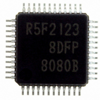
R5F21238DFP#U0
Manufacturer Part Number
R5F21238DFP#U0
Description
IC R8C/23 MCU FLASH 48-LQFP
Manufacturer
Renesas Electronics America
Series
R8C/2x/23r
Specifications of R5F21238DFP#U0
Core Size
16/32-Bit
Program Memory Size
64KB (64K x 8)
Peripherals
POR, Voltage Detect, WDT
Core Processor
R8C
Speed
20MHz
Connectivity
CAN, I²C, LIN, SIO, SSU, UART/USART
Number Of I /o
41
Program Memory Type
FLASH
Ram Size
3K x 8
Voltage - Supply (vcc/vdd)
2.7 V ~ 5.5 V
Data Converters
A/D 12x10b
Oscillator Type
Internal
Operating Temperature
-40°C ~ 85°C
Package / Case
48-LQFP
No. Of I/o's
41
Ram Memory Size
3KB
Cpu Speed
20MHz
No. Of Timers
4
Digital Ic Case Style
LQFP
Embedded Interface Type
CAN, I2C, UART
Rohs Compliant
Yes
Cpu Family
R8C
Device Core Size
16b
Frequency (max)
20MHz
Interface Type
I2C/UART
Total Internal Ram Size
3KB
# I/os (max)
41
Number Of Timers - General Purpose
5
Operating Supply Voltage (typ)
3.3/5V
Operating Supply Voltage (max)
5.5V
Operating Supply Voltage (min)
3V
On-chip Adc
12-chx10-bit
Instruction Set Architecture
CISC
Operating Temp Range
-40C to 85C
Operating Temperature Classification
Industrial
Mounting
Surface Mount
Pin Count
48
Package Type
LQFP
Lead Free Status / RoHS Status
Lead free / RoHS Compliant
For Use With
RCDK8C - KIT DEV EVAL FOR CAN R8C/23R0K521237S000BE - KIT DEV RSK R8C/23R0E521237CPE00 - EMULATOR COMPACT R8C/20/21/22/23
Eeprom Size
-
Lead Free Status / Rohs Status
Compliant
Available stocks
Company
Part Number
Manufacturer
Quantity
Price


R8C/22 Group, R8C/23 Group
Rev.2.00 Aug 20, 2008
REJ09B0251-0200
Figure 14.102 TRDOCR Register in PWM3 Mode
Timer RD Output Control Register
b7 b6 b5 b4 b3 b2
NOTES:
1.
2. When the pin functions are w aveform output (refer to Table 14.12 and 14.13) and the TRDOCR register is set, the
Write to the TRDOCR register w hen both the TSTART0 and TSTART1 bits in the TRDSTR register are set to 0 (count
stops).
initial output level is output.
b1 b0
Bit Symbol
TRDOCR
Symbol
TOA0
TOB0
TOC0
TOD0
TOA1
TOB1
TOC1
TOD1
Page 252 of 501
TRDIOA0 output level
selection bit
TRDIOB0 output level
selection bit
TRDIOC0 initial output level
selection bit
TRDIOD0 initial output level
selection bit
TRDIOA1 initial output level
selection bit
TRDIOB1 initial output level
selection bit
TRDIOC1 initial output level
selection bit
TRDIOD1 initial output level
selection bit
(1)
Address
Bit Name
013Dh
(2)
(2)
0 : Active level “H”,
1 : Active level “L”,
0 : Active level “H”,
1 : Active level “L”,
This bit is disabled in PWM3 mode.
initial output “L”,
output “H” by the compare match in the
TRDGRA1register,
output “L” by the compare match in the
TRDGRA0 register
initial output “H”,
output “L” by the compare match in the
TRDGRA1register,
output “H” by the compare match in the
TRDGRA0 register
initial output “L”,
output “H” by the compare match in the
TRDGRB1register,
output “L” by the compare match in the
TRDGRB0 register
initial output “H”,
output “L” by the compare match in the
TRDGRB1register,
output “H” by the compare match in the
TRDGRB0 register
After Reset
Function
00h
14. Timers
RW
RW
RW
RW
RW
RW
RW
RW
RW
Related parts for R5F21238DFP#U0
Image
Part Number
Description
Manufacturer
Datasheet
Request
R

Part Number:
Description:
KIT STARTER FOR M16C/29
Manufacturer:
Renesas Electronics America
Datasheet:

Part Number:
Description:
KIT STARTER FOR R8C/2D
Manufacturer:
Renesas Electronics America
Datasheet:

Part Number:
Description:
R0K33062P STARTER KIT
Manufacturer:
Renesas Electronics America
Datasheet:

Part Number:
Description:
KIT STARTER FOR R8C/23 E8A
Manufacturer:
Renesas Electronics America
Datasheet:

Part Number:
Description:
KIT STARTER FOR R8C/25
Manufacturer:
Renesas Electronics America
Datasheet:

Part Number:
Description:
KIT STARTER H8S2456 SHARPE DSPLY
Manufacturer:
Renesas Electronics America
Datasheet:

Part Number:
Description:
KIT STARTER FOR R8C38C
Manufacturer:
Renesas Electronics America
Datasheet:

Part Number:
Description:
KIT STARTER FOR R8C35C
Manufacturer:
Renesas Electronics America
Datasheet:

Part Number:
Description:
KIT STARTER FOR R8CL3AC+LCD APPS
Manufacturer:
Renesas Electronics America
Datasheet:
Part Number:
Description:
KIT STARTER FOR RX610
Manufacturer:
Renesas Electronics America
Datasheet:

Part Number:
Description:
KIT STARTER FOR R32C/118
Manufacturer:
Renesas Electronics America
Datasheet:

Part Number:
Description:
KIT DEV RSK-R8C/26-29
Manufacturer:
Renesas Electronics America
Datasheet:

Part Number:
Description:
KIT STARTER FOR SH7124
Manufacturer:
Renesas Electronics America
Datasheet:

Part Number:
Description:
KIT STARTER FOR H8SX/1622
Manufacturer:
Renesas Electronics America
Datasheet:

Part Number:
Description:
KIT DEV FOR SH7203
Manufacturer:
Renesas Electronics America
Datasheet: