DF2372RVFQ34V Renesas Electronics America, DF2372RVFQ34V Datasheet - Page 31
DF2372RVFQ34V
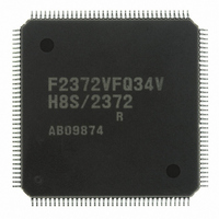
Manufacturer Part Number
DF2372RVFQ34V
Description
IC H8S/2372 MCU FLASH 144LQFP
Manufacturer
Renesas Electronics America
Series
H8® H8S/2300r
Datasheet
1.YR0K42378FC000BA.pdf
(1208 pages)
Specifications of DF2372RVFQ34V
Core Processor
H8S/2000
Core Size
16-Bit
Speed
34MHz
Connectivity
I²C, IrDA, SCI, SmartCard
Peripherals
DMA, POR, PWM, WDT
Number Of I /o
96
Program Memory Size
256KB (256K x 8)
Program Memory Type
FLASH
Ram Size
32K x 8
Voltage - Supply (vcc/vdd)
3 V ~ 3.6 V
Data Converters
A/D 16x10b; D/A 6x8b
Oscillator Type
External
Operating Temperature
-20°C ~ 75°C
Package / Case
144-LQFP
For Use With
YLCDRSK2378 - KIT DEV EVAL H8S/2378 LCDYR0K42378FC000BA - KIT EVAL FOR H8S/2378HS0005KCU11H - EMULATOR E10A-USB H8S(X),SH2(A)
Lead Free Status / RoHS Status
Lead free / RoHS Compliant
Eeprom Size
-
Available stocks
Company
Part Number
Manufacturer
Quantity
Price
Company:

Part Number:
DF2372RVFQ34V
Manufacturer:
Renesas Electronics America
Quantity:
10 000


8.5
8.6
Section 9 Data Transfer Controller (DTC) ........................................................425
9.1
9.2
9.3
9.4
9.5
9.6
8.4.6
8.4.7
8.4.8
8.4.9
8.4.10 EXDMAC Bus Cycles (Single Address Mode) .................................................... 400
8.4.11 Examples of Operation Timing in Each Mode...................................................... 405
8.4.12 Ending DMA Transfer .......................................................................................... 418
8.4.13 Relationship between EXDMAC and Other Bus Masters .................................... 419
Interrupt Sources ................................................................................................................ 420
Usage Notes ....................................................................................................................... 422
8.6.1
8.6.2
8.6.3
8.6.4
8.6.5
8.6.6
Features .............................................................................................................................. 425
Register Descriptions ......................................................................................................... 427
9.2.1
9.2.2
9.2.3
9.2.4
9.2.5
9.2.6
9.2.7
9.2.8
Activation Sources ............................................................................................................. 432
Location of Register Information and DTC Vector Table ................................................. 433
Operation............................................................................................................................ 437
9.5.1
9.5.2
9.5.3
9.5.4
9.5.5
9.5.6
9.5.7
Procedures for Using DTC................................................................................................. 447
9.6.1
9.6.2
Repeat Area Function ........................................................................................... 383
Registers during DMA Transfer Operation........................................................... 385
Channel Priority Order.......................................................................................... 390
EXDMAC Bus Cycles (Dual Address Mode)....................................................... 393
EXDMAC Register Access during Operation ...................................................... 422
Module Stop State................................................................................................. 422
EDREQ Pin Falling Edge Activation.................................................................... 422
Activation Source Acceptance .............................................................................. 423
Enabling Interrupt Requests when IRF = 1 in EDMDR ....................................... 423
ETEND Pin and CBR Refresh Cycle.................................................................... 423
DTC Mode Register A (MRA) ............................................................................. 427
DTC Mode Register B (MRB).............................................................................. 429
DTC Source Address Register (SAR)................................................................... 429
DTC Destination Address Register (DAR)........................................................... 429
DTC Transfer Count Register A (CRA) ............................................................... 430
DTC Transfer Count Register B (CRB)................................................................ 430
DTC Enable Registers A to H (DTCERA to DTCERH) ...................................... 430
DTC Vector Register (DTVECR)......................................................................... 431
Normal Mode........................................................................................................ 440
Repeat Mode ......................................................................................................... 441
Block Transfer Mode ............................................................................................ 442
Chain Transfer ...................................................................................................... 443
Interrupt Sources................................................................................................... 444
Operation Timing.................................................................................................. 444
Number of DTC Execution States ........................................................................ 445
Activation by Interrupt.......................................................................................... 447
Activation by Software ......................................................................................... 447
Rev.7.00 Mar. 18, 2009 page xxix of lxvi
REJ09B0109-0700
Related parts for DF2372RVFQ34V
Image
Part Number
Description
Manufacturer
Datasheet
Request
R

Part Number:
Description:
KIT STARTER FOR M16C/29
Manufacturer:
Renesas Electronics America
Datasheet:

Part Number:
Description:
KIT STARTER FOR R8C/2D
Manufacturer:
Renesas Electronics America
Datasheet:

Part Number:
Description:
R0K33062P STARTER KIT
Manufacturer:
Renesas Electronics America
Datasheet:

Part Number:
Description:
KIT STARTER FOR R8C/23 E8A
Manufacturer:
Renesas Electronics America
Datasheet:

Part Number:
Description:
KIT STARTER FOR R8C/25
Manufacturer:
Renesas Electronics America
Datasheet:

Part Number:
Description:
KIT STARTER H8S2456 SHARPE DSPLY
Manufacturer:
Renesas Electronics America
Datasheet:

Part Number:
Description:
KIT STARTER FOR R8C38C
Manufacturer:
Renesas Electronics America
Datasheet:

Part Number:
Description:
KIT STARTER FOR R8C35C
Manufacturer:
Renesas Electronics America
Datasheet:

Part Number:
Description:
KIT STARTER FOR R8CL3AC+LCD APPS
Manufacturer:
Renesas Electronics America
Datasheet:
Part Number:
Description:
KIT STARTER FOR RX610
Manufacturer:
Renesas Electronics America
Datasheet:

Part Number:
Description:
KIT STARTER FOR R32C/118
Manufacturer:
Renesas Electronics America
Datasheet:

Part Number:
Description:
KIT DEV RSK-R8C/26-29
Manufacturer:
Renesas Electronics America
Datasheet:

Part Number:
Description:
KIT STARTER FOR SH7124
Manufacturer:
Renesas Electronics America
Datasheet:

Part Number:
Description:
KIT STARTER FOR H8SX/1622
Manufacturer:
Renesas Electronics America
Datasheet:

Part Number:
Description:
KIT DEV FOR SH7203
Manufacturer:
Renesas Electronics America
Datasheet: