DF2372RVFQ34V Renesas Electronics America, DF2372RVFQ34V Datasheet - Page 779
DF2372RVFQ34V
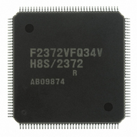
Manufacturer Part Number
DF2372RVFQ34V
Description
IC H8S/2372 MCU FLASH 144LQFP
Manufacturer
Renesas Electronics America
Series
H8® H8S/2300r
Datasheet
1.YR0K42378FC000BA.pdf
(1208 pages)
Specifications of DF2372RVFQ34V
Core Processor
H8S/2000
Core Size
16-Bit
Speed
34MHz
Connectivity
I²C, IrDA, SCI, SmartCard
Peripherals
DMA, POR, PWM, WDT
Number Of I /o
96
Program Memory Size
256KB (256K x 8)
Program Memory Type
FLASH
Ram Size
32K x 8
Voltage - Supply (vcc/vdd)
3 V ~ 3.6 V
Data Converters
A/D 16x10b; D/A 6x8b
Oscillator Type
External
Operating Temperature
-20°C ~ 75°C
Package / Case
144-LQFP
For Use With
YLCDRSK2378 - KIT DEV EVAL H8S/2378 LCDYR0K42378FC000BA - KIT EVAL FOR H8S/2378HS0005KCU11H - EMULATOR E10A-USB H8S(X),SH2(A)
Lead Free Status / RoHS Status
Lead free / RoHS Compliant
Eeprom Size
-
Available stocks
Company
Part Number
Manufacturer
Quantity
Price
Company:

Part Number:
DF2372RVFQ34V
Manufacturer:
Renesas Electronics America
Quantity:
10 000


15.3.9
BRR is an 8-bit register that adjusts the bit rate. As the SCI performs baud rate generator control
independently for each channel, different bit rates can be set for each channel. Table 15.2 shows
the relationships between the N setting in BRR and bit rate B for normal asynchronous mode,
clocked synchronous mode, and Smart Card interface mode. The initial value of BRR is H'FF, and
it can be read or written to by the CPU at all times.
Table 15.2 Relationships between N Setting in BRR and Bit Rate B
Mode
Asynchronous
Mode
Clocked
Synchronous
Mode
Smart Card
Interface Mode
Note: B: Bit rate (bit/s)
0
0
1
1
Table 15.3 shows sample N settings in BRR in normal asynchronous mode. Table 15.4 shows the
maximum bit rate for each frequency in normal asynchronous mode. Table 15.6 shows sample N
settings in BRR in clocked synchronous mode. Table 15.8 shows sample N settings in BRR in
Smart Card interface mode. In Smart Card interface mode, S (the number of basic clock periods in
a 1-bit transfer interval) can be selected. For details, refer to section 15.7.4, Receive Data
Sampling Timing and Reception Margin. Tables 15.5 and 15.7 show the maximum bit rates with
external clock input.
CKS1
N: BRR setting for baud rate generator (0 ≤ N ≤ 255)
φ: Operating frequency (MHz)
n and S: Determined by the SMR settings shown in the following tables.
SMR Setting
Bit Rate Register (BRR)
0
1
0
1
CKS0
Bit Rate
B =
B =
B =
64 × 2
S × 2
8 × 2
2n−1
2n+1
φ × 10
φ × 10
φ × 10
2n−1
0
1
2
3
n
× (N + 1)
× (N + 1)
× (N + 1)
6
6
6
Section 15 Serial Communication Interface (SCI, IrDA)
Error
Error (%) = {
Error (%) = {
0
0
1
1
BCP1
Rev.7.00 Mar. 18, 2009 page 711 of 1136
B × 64 × 2
B × S × 2
SMR Setting
0
1
0
1
BCP0
φ × 10
φ × 10
2n+1
2n−1
6
6
× (N + 1)
× (N + 1)
REJ09B0109-0700
32
64
372
256
S
− 1 } × 100
− 1 } × 100
Related parts for DF2372RVFQ34V
Image
Part Number
Description
Manufacturer
Datasheet
Request
R

Part Number:
Description:
KIT STARTER FOR M16C/29
Manufacturer:
Renesas Electronics America
Datasheet:

Part Number:
Description:
KIT STARTER FOR R8C/2D
Manufacturer:
Renesas Electronics America
Datasheet:

Part Number:
Description:
R0K33062P STARTER KIT
Manufacturer:
Renesas Electronics America
Datasheet:

Part Number:
Description:
KIT STARTER FOR R8C/23 E8A
Manufacturer:
Renesas Electronics America
Datasheet:

Part Number:
Description:
KIT STARTER FOR R8C/25
Manufacturer:
Renesas Electronics America
Datasheet:

Part Number:
Description:
KIT STARTER H8S2456 SHARPE DSPLY
Manufacturer:
Renesas Electronics America
Datasheet:

Part Number:
Description:
KIT STARTER FOR R8C38C
Manufacturer:
Renesas Electronics America
Datasheet:

Part Number:
Description:
KIT STARTER FOR R8C35C
Manufacturer:
Renesas Electronics America
Datasheet:

Part Number:
Description:
KIT STARTER FOR R8CL3AC+LCD APPS
Manufacturer:
Renesas Electronics America
Datasheet:
Part Number:
Description:
KIT STARTER FOR RX610
Manufacturer:
Renesas Electronics America
Datasheet:

Part Number:
Description:
KIT STARTER FOR R32C/118
Manufacturer:
Renesas Electronics America
Datasheet:

Part Number:
Description:
KIT DEV RSK-R8C/26-29
Manufacturer:
Renesas Electronics America
Datasheet:

Part Number:
Description:
KIT STARTER FOR SH7124
Manufacturer:
Renesas Electronics America
Datasheet:

Part Number:
Description:
KIT STARTER FOR H8SX/1622
Manufacturer:
Renesas Electronics America
Datasheet:

Part Number:
Description:
KIT DEV FOR SH7203
Manufacturer:
Renesas Electronics America
Datasheet: