DF2372RVFQ34V Renesas Electronics America, DF2372RVFQ34V Datasheet - Page 321
DF2372RVFQ34V
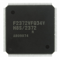
Manufacturer Part Number
DF2372RVFQ34V
Description
IC H8S/2372 MCU FLASH 144LQFP
Manufacturer
Renesas Electronics America
Series
H8® H8S/2300r
Datasheet
1.YR0K42378FC000BA.pdf
(1208 pages)
Specifications of DF2372RVFQ34V
Core Processor
H8S/2000
Core Size
16-Bit
Speed
34MHz
Connectivity
I²C, IrDA, SCI, SmartCard
Peripherals
DMA, POR, PWM, WDT
Number Of I /o
96
Program Memory Size
256KB (256K x 8)
Program Memory Type
FLASH
Ram Size
32K x 8
Voltage - Supply (vcc/vdd)
3 V ~ 3.6 V
Data Converters
A/D 16x10b; D/A 6x8b
Oscillator Type
External
Operating Temperature
-20°C ~ 75°C
Package / Case
144-LQFP
For Use With
YLCDRSK2378 - KIT DEV EVAL H8S/2378 LCDYR0K42378FC000BA - KIT EVAL FOR H8S/2378HS0005KCU11H - EMULATOR E10A-USB H8S(X),SH2(A)
Lead Free Status / RoHS Status
Lead free / RoHS Compliant
Eeprom Size
-
Available stocks
Company
Part Number
Manufacturer
Quantity
Price
Company:

Part Number:
DF2372RVFQ34V
Manufacturer:
Renesas Electronics America
Quantity:
10 000


Idle Cycle in Case of DRAM Space Access after Normal Space Access: In a DRAM space
access following a normal space access, the settings of bits ICIS2, ICIS1, ICIS0, and IDLC in
BCR are valid. However, in the case of consecutive reads in different areas, for example, if the
second read is a full access to DRAM space, only a T
timing in this case is shown in figure 6.69.
In burst access in RAS down mode, the settings of bits ICIS2, ICIS1, ICIS0, and IDLC are valid
and an idle cycle is inserted. The timing in this case is illustrated in figures 6.70 and 6.71.
Figure 6.69 Example of DRAM Full Access after External Read
Address bus
Data bus
RD
φ
T
1
External read
T
2
(CAST = 0)
T
3
p
T
p
cycle is inserted, and a T
Rev.7.00 Mar. 18, 2009 page 253 of 1136
DRAM space read
T
r
T
Section 6 Bus Controller (BSC)
c1
T
c2
i
REJ09B0109-0700
cycle is not. The
Related parts for DF2372RVFQ34V
Image
Part Number
Description
Manufacturer
Datasheet
Request
R

Part Number:
Description:
KIT STARTER FOR M16C/29
Manufacturer:
Renesas Electronics America
Datasheet:

Part Number:
Description:
KIT STARTER FOR R8C/2D
Manufacturer:
Renesas Electronics America
Datasheet:

Part Number:
Description:
R0K33062P STARTER KIT
Manufacturer:
Renesas Electronics America
Datasheet:

Part Number:
Description:
KIT STARTER FOR R8C/23 E8A
Manufacturer:
Renesas Electronics America
Datasheet:

Part Number:
Description:
KIT STARTER FOR R8C/25
Manufacturer:
Renesas Electronics America
Datasheet:

Part Number:
Description:
KIT STARTER H8S2456 SHARPE DSPLY
Manufacturer:
Renesas Electronics America
Datasheet:

Part Number:
Description:
KIT STARTER FOR R8C38C
Manufacturer:
Renesas Electronics America
Datasheet:

Part Number:
Description:
KIT STARTER FOR R8C35C
Manufacturer:
Renesas Electronics America
Datasheet:

Part Number:
Description:
KIT STARTER FOR R8CL3AC+LCD APPS
Manufacturer:
Renesas Electronics America
Datasheet:
Part Number:
Description:
KIT STARTER FOR RX610
Manufacturer:
Renesas Electronics America
Datasheet:

Part Number:
Description:
KIT STARTER FOR R32C/118
Manufacturer:
Renesas Electronics America
Datasheet:

Part Number:
Description:
KIT DEV RSK-R8C/26-29
Manufacturer:
Renesas Electronics America
Datasheet:

Part Number:
Description:
KIT STARTER FOR SH7124
Manufacturer:
Renesas Electronics America
Datasheet:

Part Number:
Description:
KIT STARTER FOR H8SX/1622
Manufacturer:
Renesas Electronics America
Datasheet:

Part Number:
Description:
KIT DEV FOR SH7203
Manufacturer:
Renesas Electronics America
Datasheet: