DF2372RVFQ34V Renesas Electronics America, DF2372RVFQ34V Datasheet - Page 554
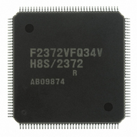
DF2372RVFQ34V
Manufacturer Part Number
DF2372RVFQ34V
Description
IC H8S/2372 MCU FLASH 144LQFP
Manufacturer
Renesas Electronics America
Series
H8® H8S/2300r
Datasheet
1.YR0K42378FC000BA.pdf
(1208 pages)
Specifications of DF2372RVFQ34V
Core Processor
H8S/2000
Core Size
16-Bit
Speed
34MHz
Connectivity
I²C, IrDA, SCI, SmartCard
Peripherals
DMA, POR, PWM, WDT
Number Of I /o
96
Program Memory Size
256KB (256K x 8)
Program Memory Type
FLASH
Ram Size
32K x 8
Voltage - Supply (vcc/vdd)
3 V ~ 3.6 V
Data Converters
A/D 16x10b; D/A 6x8b
Oscillator Type
External
Operating Temperature
-20°C ~ 75°C
Package / Case
144-LQFP
For Use With
YLCDRSK2378 - KIT DEV EVAL H8S/2378 LCDYR0K42378FC000BA - KIT EVAL FOR H8S/2378HS0005KCU11H - EMULATOR E10A-USB H8S(X),SH2(A)
Lead Free Status / RoHS Status
Lead free / RoHS Compliant
Eeprom Size
-
Available stocks
Company
Part Number
Manufacturer
Quantity
Price
Company:

Part Number:
DF2372RVFQ34V
Manufacturer:
Renesas Electronics America
Quantity:
10 000


Section 10 I/O Ports
10.3.6
Port 3 pins also function as the pins for SCI I/Os, I
correspondence between the register specification and the pin functions is shown below.
• P35/SCK1/SCL0/(OE)/(CKE *
OEE
OES
SDRAM
space
ICE
CKE1
C/A
CKE0
P35DDR
Pin
function
Rev.7.00 Mar. 18, 2009 page 486 of 1136
REJ09B0109-0700
The pin function is switched as shown below according to the combination of the ICE bit in
ICCRA of I
RMTS2 to RMTS0 in DRAMCR, bit OES in PFCR2, and bit P35DDR.
Modes 1, 2, 4, 7 (EXPE = 1)
Pin Functions
input
P35
0
0
2
C_0, C/A bit in SMR of SCI_1, bits CKE0 and CKE1 in SCR, bits OEE and
output
P35
*
0
1
1
0
output
SCK1
⎯
⎯
*
1
1
⎯
⎯
0
output
SCK1
⎯
⎯
*
1
1
3
)
SCK1
input
⎯
⎯
⎯
1
SCL0
I/O *
⎯
⎯
⎯
⎯
1
2
input
P35
0
2
C output, and a bus control signal output. The
0
output
P35
*
0
1
1
0
output
SCK1
⎯
*
0
1
1
⎯
1
output
SCK1
⎯
⎯
*
1
1
1
SCK1
input
⎯
⎯
⎯
1
SCL0
I/O *
⎯
⎯
⎯
⎯
1
2
Normal
DRAM
output
space
OE
or
⎯
⎯
⎯
⎯
⎯
0
continu-
SDRAM
output
space
CKE
ous
⎯
⎯
⎯
⎯
⎯
Related parts for DF2372RVFQ34V
Image
Part Number
Description
Manufacturer
Datasheet
Request
R

Part Number:
Description:
KIT STARTER FOR M16C/29
Manufacturer:
Renesas Electronics America
Datasheet:

Part Number:
Description:
KIT STARTER FOR R8C/2D
Manufacturer:
Renesas Electronics America
Datasheet:

Part Number:
Description:
R0K33062P STARTER KIT
Manufacturer:
Renesas Electronics America
Datasheet:

Part Number:
Description:
KIT STARTER FOR R8C/23 E8A
Manufacturer:
Renesas Electronics America
Datasheet:

Part Number:
Description:
KIT STARTER FOR R8C/25
Manufacturer:
Renesas Electronics America
Datasheet:

Part Number:
Description:
KIT STARTER H8S2456 SHARPE DSPLY
Manufacturer:
Renesas Electronics America
Datasheet:

Part Number:
Description:
KIT STARTER FOR R8C38C
Manufacturer:
Renesas Electronics America
Datasheet:

Part Number:
Description:
KIT STARTER FOR R8C35C
Manufacturer:
Renesas Electronics America
Datasheet:

Part Number:
Description:
KIT STARTER FOR R8CL3AC+LCD APPS
Manufacturer:
Renesas Electronics America
Datasheet:
Part Number:
Description:
KIT STARTER FOR RX610
Manufacturer:
Renesas Electronics America
Datasheet:

Part Number:
Description:
KIT STARTER FOR R32C/118
Manufacturer:
Renesas Electronics America
Datasheet:

Part Number:
Description:
KIT DEV RSK-R8C/26-29
Manufacturer:
Renesas Electronics America
Datasheet:

Part Number:
Description:
KIT STARTER FOR SH7124
Manufacturer:
Renesas Electronics America
Datasheet:

Part Number:
Description:
KIT STARTER FOR H8SX/1622
Manufacturer:
Renesas Electronics America
Datasheet:

Part Number:
Description:
KIT DEV FOR SH7203
Manufacturer:
Renesas Electronics America
Datasheet: