DF2372RVFQ34V Renesas Electronics America, DF2372RVFQ34V Datasheet - Page 65
DF2372RVFQ34V
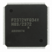
Manufacturer Part Number
DF2372RVFQ34V
Description
IC H8S/2372 MCU FLASH 144LQFP
Manufacturer
Renesas Electronics America
Series
H8® H8S/2300r
Datasheet
1.YR0K42378FC000BA.pdf
(1208 pages)
Specifications of DF2372RVFQ34V
Core Processor
H8S/2000
Core Size
16-Bit
Speed
34MHz
Connectivity
I²C, IrDA, SCI, SmartCard
Peripherals
DMA, POR, PWM, WDT
Number Of I /o
96
Program Memory Size
256KB (256K x 8)
Program Memory Type
FLASH
Ram Size
32K x 8
Voltage - Supply (vcc/vdd)
3 V ~ 3.6 V
Data Converters
A/D 16x10b; D/A 6x8b
Oscillator Type
External
Operating Temperature
-20°C ~ 75°C
Package / Case
144-LQFP
For Use With
YLCDRSK2378 - KIT DEV EVAL H8S/2378 LCDYR0K42378FC000BA - KIT EVAL FOR H8S/2378HS0005KCU11H - EMULATOR E10A-USB H8S(X),SH2(A)
Lead Free Status / RoHS Status
Lead free / RoHS Compliant
Eeprom Size
-
Available stocks
Company
Part Number
Manufacturer
Quantity
Price
Company:

Part Number:
DF2372RVFQ34V
Manufacturer:
Renesas Electronics America
Quantity:
10 000


Section 16 I
Table 16.1
Table 16.2
Table 16.3
Table 16.4
Section 17 A/D Converter..................................................................................805
Table 17.1
Table 17.2
Table 17.3
Table 17.4
Table 17.5
Table 17.6
Section 18 D/A Converter..................................................................................821
Table 18.1
Table 18.2
Table 18.3
Table 18.4
Section 19 RAM ................................................................................................831
Section 20 Flash Memory (0.35-μm F-ZTAT Version) ....................................833
Table 20.1
Table 20.2
Table 20.3
Table 20.4
Table 20.5
Table 20.6
Table 20.7
Section 21 Flash Memory (0.18-μm F-ZTAT Version) ....................................861
Table 21.1
Table 21.2
Table 21.3
Table 21.4
Table 21.5
Table 21.6
Table 21.7
Table 21.8 (1) Useable Area for Programming in User Program Mode ....................................... 912
Pin Configuration .................................................................................................... 773
Transfer Rate ........................................................................................................... 776
Interrupt Requests ................................................................................................... 801
Time for monitoring SCL........................................................................................ 802
Pin Configuration .................................................................................................... 807
Analog Input Channels and Corresponding ADDR Registers................................. 808
A/D Conversion Time (Single Mode) ..................................................................... 814
A/D Conversion Time (Scan Mode)........................................................................ 815
A/D Converter Interrupt Source .............................................................................. 816
Analog Pin Specifications ....................................................................................... 820
Pin Configuration .................................................................................................... 824
Control of D/A Conversion ..................................................................................... 826
Control of D/A Conversion ..................................................................................... 827
Control of D/A Conversion ..................................................................................... 828
Differences between Boot Mode and User Program Mode..................................... 835
Pin Configuration .................................................................................................... 840
Erase Blocks............................................................................................................ 845
Setting On-Board Programming Mode ................................................................... 846
Boot Mode Operation.............................................................................................. 848
System Clock Frequencies for which Automatic Adjustment
of LSI Bit Rate Is Possible ...................................................................................... 849
Flash Memory Operating States .............................................................................. 855
Comparison of Programming Modes ...................................................................... 865
Pin Configuration .................................................................................................... 870
Register/Parameter and Target Mode...................................................................... 872
Parameters and Target Modes ................................................................................. 880
Setting On-Board Programming Mode ................................................................... 891
System Clock Frequency for Automatic-Bit-Rate Adjustment by This LSI ........... 893
Executable MAT ..................................................................................................... 911
2
C Bus Interface 2 (IIC2) (Option) .................................................771
Rev.7.00 Mar. 18, 2009 page lxiii of lxvi
REJ09B0109-0700
Related parts for DF2372RVFQ34V
Image
Part Number
Description
Manufacturer
Datasheet
Request
R

Part Number:
Description:
KIT STARTER FOR M16C/29
Manufacturer:
Renesas Electronics America
Datasheet:

Part Number:
Description:
KIT STARTER FOR R8C/2D
Manufacturer:
Renesas Electronics America
Datasheet:

Part Number:
Description:
R0K33062P STARTER KIT
Manufacturer:
Renesas Electronics America
Datasheet:

Part Number:
Description:
KIT STARTER FOR R8C/23 E8A
Manufacturer:
Renesas Electronics America
Datasheet:

Part Number:
Description:
KIT STARTER FOR R8C/25
Manufacturer:
Renesas Electronics America
Datasheet:

Part Number:
Description:
KIT STARTER H8S2456 SHARPE DSPLY
Manufacturer:
Renesas Electronics America
Datasheet:

Part Number:
Description:
KIT STARTER FOR R8C38C
Manufacturer:
Renesas Electronics America
Datasheet:

Part Number:
Description:
KIT STARTER FOR R8C35C
Manufacturer:
Renesas Electronics America
Datasheet:

Part Number:
Description:
KIT STARTER FOR R8CL3AC+LCD APPS
Manufacturer:
Renesas Electronics America
Datasheet:
Part Number:
Description:
KIT STARTER FOR RX610
Manufacturer:
Renesas Electronics America
Datasheet:

Part Number:
Description:
KIT STARTER FOR R32C/118
Manufacturer:
Renesas Electronics America
Datasheet:

Part Number:
Description:
KIT DEV RSK-R8C/26-29
Manufacturer:
Renesas Electronics America
Datasheet:

Part Number:
Description:
KIT STARTER FOR SH7124
Manufacturer:
Renesas Electronics America
Datasheet:

Part Number:
Description:
KIT STARTER FOR H8SX/1622
Manufacturer:
Renesas Electronics America
Datasheet:

Part Number:
Description:
KIT DEV FOR SH7203
Manufacturer:
Renesas Electronics America
Datasheet: