DF2372RVFQ34V Renesas Electronics America, DF2372RVFQ34V Datasheet - Page 835
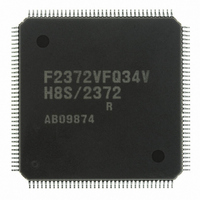
DF2372RVFQ34V
Manufacturer Part Number
DF2372RVFQ34V
Description
IC H8S/2372 MCU FLASH 144LQFP
Manufacturer
Renesas Electronics America
Series
H8® H8S/2300r
Datasheet
1.YR0K42378FC000BA.pdf
(1208 pages)
Specifications of DF2372RVFQ34V
Core Processor
H8S/2000
Core Size
16-Bit
Speed
34MHz
Connectivity
I²C, IrDA, SCI, SmartCard
Peripherals
DMA, POR, PWM, WDT
Number Of I /o
96
Program Memory Size
256KB (256K x 8)
Program Memory Type
FLASH
Ram Size
32K x 8
Voltage - Supply (vcc/vdd)
3 V ~ 3.6 V
Data Converters
A/D 16x10b; D/A 6x8b
Oscillator Type
External
Operating Temperature
-20°C ~ 75°C
Package / Case
144-LQFP
For Use With
YLCDRSK2378 - KIT DEV EVAL H8S/2378 LCDYR0K42378FC000BA - KIT EVAL FOR H8S/2378HS0005KCU11H - EMULATOR E10A-USB H8S(X),SH2(A)
Lead Free Status / RoHS Status
Lead free / RoHS Compliant
Eeprom Size
-
Available stocks
Company
Part Number
Manufacturer
Quantity
Price
Company:

Part Number:
DF2372RVFQ34V
Manufacturer:
Renesas Electronics America
Quantity:
10 000


15.10.7 Operation in Case of Mode Transition
• Transmission
• Reception
Operation should be stopped (by clearing TE, TIE, and TEIE to 0) before making a module
stop mode or software standby mode transition. TSR, TDR, and SSR are reset. The output pin
states in module stop mode or software standby mode depend on the port settings, and become
high-level output after the relevant mode is cleared. If a transition is made during transmission,
the data being transmitted will be undefined.
When transmitting without changing the transmit mode after the relevant mode is cleared,
transmission can be started by setting TE to 1 again, and performing the following sequence:
SSR read → TDR write → TDRE clearance. To transmit with a different transmit mode after
clearing the relevant mode, the procedure must be started again from initialization.
Figure 15.36 shows a sample flowchart for mode transition during transmission. Port pin states
during mode transition are shown in figures 15.37 and 15.38.
Operation should also be stopped (by clearing TE, TIE, and TEIE to 0) before making a
transition from transmission by DTC transfer to module stop mode or software standby mode
transition. To perform transmission with the DTC after the relevant mode is cleared, setting TE
and TIE to 1 will set the TXI flag and start DTC transmission.
Receive operation should be stopped (by clearing RE to 0) before making a module stop mode
or software standby mode transition. RSR, RDR, and SSR are reset. If a transition is made
during reception, the data being received will be invalid.
To continue receiving without changing the reception mode after the relevant mode is cleared,
set RE to 1 before starting reception. To receive with a different receive mode, the procedure
must be started again from initialization.
Section 15 Serial Communication Interface (SCI, IrDA)
Rev.7.00 Mar. 18, 2009 page 767 of 1136
REJ09B0109-0700
Related parts for DF2372RVFQ34V
Image
Part Number
Description
Manufacturer
Datasheet
Request
R

Part Number:
Description:
KIT STARTER FOR M16C/29
Manufacturer:
Renesas Electronics America
Datasheet:

Part Number:
Description:
KIT STARTER FOR R8C/2D
Manufacturer:
Renesas Electronics America
Datasheet:

Part Number:
Description:
R0K33062P STARTER KIT
Manufacturer:
Renesas Electronics America
Datasheet:

Part Number:
Description:
KIT STARTER FOR R8C/23 E8A
Manufacturer:
Renesas Electronics America
Datasheet:

Part Number:
Description:
KIT STARTER FOR R8C/25
Manufacturer:
Renesas Electronics America
Datasheet:

Part Number:
Description:
KIT STARTER H8S2456 SHARPE DSPLY
Manufacturer:
Renesas Electronics America
Datasheet:

Part Number:
Description:
KIT STARTER FOR R8C38C
Manufacturer:
Renesas Electronics America
Datasheet:

Part Number:
Description:
KIT STARTER FOR R8C35C
Manufacturer:
Renesas Electronics America
Datasheet:

Part Number:
Description:
KIT STARTER FOR R8CL3AC+LCD APPS
Manufacturer:
Renesas Electronics America
Datasheet:
Part Number:
Description:
KIT STARTER FOR RX610
Manufacturer:
Renesas Electronics America
Datasheet:

Part Number:
Description:
KIT STARTER FOR R32C/118
Manufacturer:
Renesas Electronics America
Datasheet:

Part Number:
Description:
KIT DEV RSK-R8C/26-29
Manufacturer:
Renesas Electronics America
Datasheet:

Part Number:
Description:
KIT STARTER FOR SH7124
Manufacturer:
Renesas Electronics America
Datasheet:

Part Number:
Description:
KIT STARTER FOR H8SX/1622
Manufacturer:
Renesas Electronics America
Datasheet:

Part Number:
Description:
KIT DEV FOR SH7203
Manufacturer:
Renesas Electronics America
Datasheet: