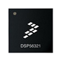
XC56309VL100A Freescale Semiconductor, XC56309VL100A Datasheet - Page 126

XC56309VL100A
Manufacturer Part Number
XC56309VL100A
Description
IC DSP 24BIT 100MHZ 196-MAPBGA
Manufacturer
Freescale Semiconductor
Series
DSP563xxr
Type
Fixed Pointr
Specifications of XC56309VL100A
Interface
Host Interface, SSI, SCI
Clock Rate
100MHz
Non-volatile Memory
ROM (576 B)
On-chip Ram
24kB
Voltage - I/o
3.30V
Voltage - Core
3.30V
Operating Temperature
-40°C ~ 100°C
Mounting Type
Surface Mount
Package / Case
196-MAPBGA
Device Core Size
24b
Format
Fixed Point
Clock Freq (max)
100MHz
Mips
100
Device Input Clock Speed
100MHz
Ram Size
102KB
Operating Supply Voltage (typ)
3.3V
Operating Supply Voltage (min)
3V
Operating Supply Voltage (max)
3.6V
Operating Temp Range
-40C to 100C
Operating Temperature Classification
Industrial
Mounting
Surface Mount
Pin Count
196
Package Type
MA-BGA
Lead Free Status / RoHS Status
Lead free / RoHS Compliant
Available stocks
Company
Part Number
Manufacturer
Quantity
Price
Company:
Part Number:
XC56309VL100A
Manufacturer:
Freescale Semiconductor
Quantity:
10 000
Company:
Part Number:
XC56309VL100AR2
Manufacturer:
Freescale Semiconductor
Quantity:
10 000
- Current page: 126 of 284
- Download datasheet (4Mb)
Host Interface (HI08)
6.7.4 Interrupt Vector Register (IVR)
The IVR is an 8-bit read/write register that typically contains the interrupt vector number used
with MC68000 family processor vectored interrupts. Only the host processor can read and write
this register. The contents of the IVR are placed on the host data bus, H[7–0], when both the
HREQ
hardware or software reset. This value corresponds to the uninitialized interrupt vector in the
MC68000 family.
6.7.5 Receive Data Registers (RXH:RXM:RXL)
The host processor views the receive byte registers as three 8-bit read-only registers: the receive
high register (RXH), the receive middle register (RXM), and the receive low register (RXL).
They receive data from the high, middle, and low bytes, respectively, of the HTX register and are
selected by the external host address inputs (HA[2–0]) during a host processor read operation.
The memory address of the receive byte registers are set by ICR[HLEND]. If ICR[HLEND] is
set, the RXH is located at address $7, RXM at $6, and RXL at $5. If ICR[HLEND] is cleared, the
RXH is located at address $5, RXM at $6, and RXL at $7.
When data is transferred from the HTX register to the receive byte register at host address $7, the
ISR Receive Data Register Full (RXDF) bit is set. The host processor can program the RREQ bit
to assert the external HREQ signal when ISR[RXDF] is set. This indicates that the HI08 has a full
word (either 8, 16, or 24 bits) for the host processor. The host processor can program the RREQ
bit to assert the external HREQ signal when ISR[RXDF] is set. Assertion of the HREQ signal
informs the host processor that the receive byte registers have data to be read. When the host
reads the receive byte register at host address $7, the ISR[RXDF] bit is cleared.
6-26
Bit Number
and
0
HACK
Table 6-17. Interface Status Register (ISR) Bit Definitions (Continued)
Bit Name
signals are asserted. The contents of this register are initialized to $0F by a
RXDF
IV7
Figure 6-18. Interrupt Vector Register (IVR)
7
Reset Value
0
IV6
6
DSP56309 User’s Manual, Rev. 1
IV5
5
Receive Data Register Full
Indicates that the receive byte registers (RXH:RXM:RXL) contain data
from the DSP56309 to be read by the host processor. RXDF is set when
the HTX is transferred to the receive byte registers. RXDF is cleared
when the host processor reads the receive data register (RXL or RXH
according to HLEND bit). The host processor can clear RXDF using the
initialize function. RXDF can assert the external HREQ signal if the
RREQ bit is set. Regardless of whether the RXDF interrupt is enabled,
RXDF indicates whether the RX registers are full and data can be
latched out (so that the host processor can use polling techniques).
IV4
4
IV3
3
IV2
2
Description
IV1
1
IV0
0
Freescale Semiconductor
Related parts for XC56309VL100A
Image
Part Number
Description
Manufacturer
Datasheet
Request
R
Part Number:
Description:
Manufacturer:
Freescale Semiconductor, Inc
Datasheet:
Part Number:
Description:
Manufacturer:
Freescale Semiconductor, Inc
Datasheet:
Part Number:
Description:
Manufacturer:
Freescale Semiconductor, Inc
Datasheet:
Part Number:
Description:
Manufacturer:
Freescale Semiconductor, Inc
Datasheet:
Part Number:
Description:
Manufacturer:
Freescale Semiconductor, Inc
Datasheet:
Part Number:
Description:
Manufacturer:
Freescale Semiconductor, Inc
Datasheet:
Part Number:
Description:
Manufacturer:
Freescale Semiconductor, Inc
Datasheet:
Part Number:
Description:
Manufacturer:
Freescale Semiconductor, Inc
Datasheet:
Part Number:
Description:
Manufacturer:
Freescale Semiconductor, Inc
Datasheet:
Part Number:
Description:
Manufacturer:
Freescale Semiconductor, Inc
Datasheet:
Part Number:
Description:
Manufacturer:
Freescale Semiconductor, Inc
Datasheet:
Part Number:
Description:
Manufacturer:
Freescale Semiconductor, Inc
Datasheet:
Part Number:
Description:
Manufacturer:
Freescale Semiconductor, Inc
Datasheet:
Part Number:
Description:
Manufacturer:
Freescale Semiconductor, Inc
Datasheet:
Part Number:
Description:
Manufacturer:
Freescale Semiconductor, Inc
Datasheet:


