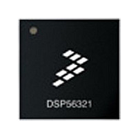
XC56309VL100A Freescale Semiconductor, XC56309VL100A Datasheet - Page 185

XC56309VL100A
Manufacturer Part Number
XC56309VL100A
Description
IC DSP 24BIT 100MHZ 196-MAPBGA
Manufacturer
Freescale Semiconductor
Series
DSP563xxr
Type
Fixed Pointr
Specifications of XC56309VL100A
Interface
Host Interface, SSI, SCI
Clock Rate
100MHz
Non-volatile Memory
ROM (576 B)
On-chip Ram
24kB
Voltage - I/o
3.30V
Voltage - Core
3.30V
Operating Temperature
-40°C ~ 100°C
Mounting Type
Surface Mount
Package / Case
196-MAPBGA
Device Core Size
24b
Format
Fixed Point
Clock Freq (max)
100MHz
Mips
100
Device Input Clock Speed
100MHz
Ram Size
102KB
Operating Supply Voltage (typ)
3.3V
Operating Supply Voltage (min)
3V
Operating Supply Voltage (max)
3.6V
Operating Temp Range
-40C to 100C
Operating Temperature Classification
Industrial
Mounting
Surface Mount
Pin Count
196
Package Type
MA-BGA
Lead Free Status / RoHS Status
Lead free / RoHS Compliant
Available stocks
Company
Part Number
Manufacturer
Quantity
Price
Company:
Part Number:
XC56309VL100A
Manufacturer:
Freescale Semiconductor
Quantity:
10 000
Company:
Part Number:
XC56309VL100AR2
Manufacturer:
Freescale Semiconductor
Quantity:
10 000
- Current page: 185 of 284
- Download datasheet (4Mb)
8.6.3 SCI Clock Control Register (SCCR)
The SCCR is a read/write register that controls the selection of clock modes and baud rates for
the transmit and receive sections of the SCI interface. The SCCR is cleared by a hardware
signal.
Freescale Semiconductor
Number
23–16
11–0
Bit
15
14
13
12
TCM
CD7
23
15
7
Bit Name
CD[11–0]
RCM
COD
TCM
SCP
Reserved. Read as 0. Write to 0 for future compatibility.
RCM
CD6
Table 8-5. SCI Clock Control Register (SCCR) Bit Definitions
22
14
6
Reset
Value
0
0
0
0
0
0
Figure 8-4. SCI Clock Control Register (SCCR)
Reserved. Write to 0 for future compatibility.
Transmit Clock Source
Selects whether an internal or external clock is used for the transmitter. If TCM is cleared,
the internal clock is used. If TCM is set, the external clock (from the SCLK signal) is used.
Receive Clock Mode Source
Selects whether an internal or external clock is used for the receiver. If RCM is cleared, the
internal clock is used. If RCM is set, the external clock (from the SCLK signal) is used.
Clock Prescaler
Selects a divide by 1 (SCP is cleared) or divide by 8 (SCP is set) prescaler for the clock
divider. The output of the prescaler is further divided by 2 to form the SCI clock.
The clock output divider is controlled by COD and the SCI mode. If the SCI mode is
synchronous, the output divider is fixed at divide by 2. If the SCI mode is asynchronous,
either:
• If COD is cleared and SCLK is an output (that is, TCM and RCM are both cleared), then
• If COD is set and SCLK is an output, the SCI clock is fed directly out to the SCLK signal.
Clock Divider
Specifies the divide ratio of the prescale divider in the SCI clock generator. A divide ratio
from 1 to 4096 (CD[11–0] = $000 to $FFF) can be selected.
Clock Out Divider
TCM
the SCI clock is divided by 16 before being output to the SCLK signal. Thus, the SCLK
output is a 1
Thus, the SCLK output is a 16
0
0
1
1
SCP
CD5
21
13
5
RCM
DSP56309 User’s Manual, Rev. 1
0
1
0
1
×
clock.
TX Clock
COD
CD4
External
External
Internal
Internal
20
12
4
RX Clock
External
External
Internal
Internal
×
CD11
CD3
baud clock.
19
11
3
Description
Output
SCLK
Input
Input
Input
CD10
CD2
18
10
2
Synchronous/asynchronous
Synchronous/asynchronous
Asynchronous only
Asynchronous only
SCI Programming Model
CD9
CD1
17
9
1
Mode
CD8
CD0
RESET
16
8
0
8-17
Related parts for XC56309VL100A
Image
Part Number
Description
Manufacturer
Datasheet
Request
R
Part Number:
Description:
Manufacturer:
Freescale Semiconductor, Inc
Datasheet:
Part Number:
Description:
Manufacturer:
Freescale Semiconductor, Inc
Datasheet:
Part Number:
Description:
Manufacturer:
Freescale Semiconductor, Inc
Datasheet:
Part Number:
Description:
Manufacturer:
Freescale Semiconductor, Inc
Datasheet:
Part Number:
Description:
Manufacturer:
Freescale Semiconductor, Inc
Datasheet:
Part Number:
Description:
Manufacturer:
Freescale Semiconductor, Inc
Datasheet:
Part Number:
Description:
Manufacturer:
Freescale Semiconductor, Inc
Datasheet:
Part Number:
Description:
Manufacturer:
Freescale Semiconductor, Inc
Datasheet:
Part Number:
Description:
Manufacturer:
Freescale Semiconductor, Inc
Datasheet:
Part Number:
Description:
Manufacturer:
Freescale Semiconductor, Inc
Datasheet:
Part Number:
Description:
Manufacturer:
Freescale Semiconductor, Inc
Datasheet:
Part Number:
Description:
Manufacturer:
Freescale Semiconductor, Inc
Datasheet:
Part Number:
Description:
Manufacturer:
Freescale Semiconductor, Inc
Datasheet:
Part Number:
Description:
Manufacturer:
Freescale Semiconductor, Inc
Datasheet:
Part Number:
Description:
Manufacturer:
Freescale Semiconductor, Inc
Datasheet:


