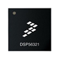
XC56309VL100A Freescale Semiconductor, XC56309VL100A Datasheet - Page 82

XC56309VL100A
Manufacturer Part Number
XC56309VL100A
Description
IC DSP 24BIT 100MHZ 196-MAPBGA
Manufacturer
Freescale Semiconductor
Series
DSP563xxr
Type
Fixed Pointr
Specifications of XC56309VL100A
Interface
Host Interface, SSI, SCI
Clock Rate
100MHz
Non-volatile Memory
ROM (576 B)
On-chip Ram
24kB
Voltage - I/o
3.30V
Voltage - Core
3.30V
Operating Temperature
-40°C ~ 100°C
Mounting Type
Surface Mount
Package / Case
196-MAPBGA
Device Core Size
24b
Format
Fixed Point
Clock Freq (max)
100MHz
Mips
100
Device Input Clock Speed
100MHz
Ram Size
102KB
Operating Supply Voltage (typ)
3.3V
Operating Supply Voltage (min)
3V
Operating Supply Voltage (max)
3.6V
Operating Temp Range
-40C to 100C
Operating Temperature Classification
Industrial
Mounting
Surface Mount
Pin Count
196
Package Type
MA-BGA
Lead Free Status / RoHS Status
Lead free / RoHS Compliant
Available stocks
Company
Part Number
Manufacturer
Quantity
Price
Company:
Part Number:
XC56309VL100A
Manufacturer:
Freescale Semiconductor
Quantity:
10 000
Company:
Part Number:
XC56309VL100AR2
Manufacturer:
Freescale Semiconductor
Quantity:
10 000
- Current page: 82 of 284
- Download datasheet (4Mb)
Core Configuration
4-24
Number
22–15
BPLE
Bit
BRP
23
14
13
23
11
Bit Name
BRF[7–0]
Reserved bit. Read as zero; write to zero for future compatibility
BRF7
BREN
BSTR
BRP
22
10
BRF6
BPS1
Table 4-9. DRAM Control Register (DCR) Bit Definitions
21
Reset
9
Value
0
0
0
0
Figure 4-7. DRAM Control Register (DCR)
BRF5
BPS0
20
Bus Refresh Prescaler
Controls a prescaler in series with the refresh clock divider. If BPR is set, a divide-by-64
prescaler is connected in series with the refresh clock divider. If BPR is cleared, the
prescaler is bypassed. The refresh request rate (in clock cycles) is the value written to
BRF[7–0] bits + 1, multiplied by 64 (if BRP is set) or by one (if BRP is cleared). When
programming the periodic refresh rate, you must consider the RAS time-out period.
Hardware support for the RAS time-out restriction does not exist
Note:
Bus Refresh Rate
Controls the refresh request rate. The BRF[7–0] bits specify a divide rate of 1–256
(BRF[7–0] = $00–$FF). A refresh request is generated each time the refresh counter
reaches zero if the refresh counter is enabled (BRE = 1).
Bus Software Triggered Reset
Generates a software-triggered refresh request. When BSTR is set, a refresh request is
generated and a refresh access is executed to all DRAM banks (the exact timing of the
refresh access depends on the pending external accesses and the status of the BME bit).
After the refresh access (CAS before RAS) is executed, the DRAM controller hardware
clears the BSTR bit. The refresh cycle length depends on the BRW[1–0] bits (a refresh
access is as long as the out-of-page access).
Bus Refresh Enable
Enables/disables the internal refresh counter. When BREN is set, the refresh counter is
enabled and a refresh request (CAS before RAS) is generated each time the refresh
counter reaches zero. A refresh cycle occurs for all DRAM banks together (that is, all pins
that are defined as RAS are asserted together). When this bit is cleared, the refresh
counter is disabled and a refresh request may be software triggered by using the BSTR
bit. In a system in which DSPs share the same DRAM, the DRAM controller of more than
one DSP may be active, but it is recommended that only one DSP have its BREN bit set
and that bus mastership is requested for a refresh access. If BREN is set and a WAIT
instruction is executed, periodic refresh is still generated each time the refresh counter
reaches zero. If BREN is set and a STOP instruction is executed, periodic refresh is not
generated and the refresh counter is disabled. The contents of the DRAM are lost.
8
BRF4
Refresh requests are not accumulated and, therefore, in a fast refresh request
rate not all the refresh requests are served (for example, the combination
BRF[7–0] = $00 and BRP = 0 generates a refresh request every clock cycle, but
a refresh access takes at least five clock cycles).
DSP56309 User’s Manual, Rev. 1
19
7
BRF3
18
6
BRF2
17
5
Description
BRF1
16
4
BRW1
BRF0
15
3
BRW0
BSTR
14
2
.
Freescale Semiconductor
BCW1
BREN
13
1
BCW0
BME
12
0
Related parts for XC56309VL100A
Image
Part Number
Description
Manufacturer
Datasheet
Request
R
Part Number:
Description:
Manufacturer:
Freescale Semiconductor, Inc
Datasheet:
Part Number:
Description:
Manufacturer:
Freescale Semiconductor, Inc
Datasheet:
Part Number:
Description:
Manufacturer:
Freescale Semiconductor, Inc
Datasheet:
Part Number:
Description:
Manufacturer:
Freescale Semiconductor, Inc
Datasheet:
Part Number:
Description:
Manufacturer:
Freescale Semiconductor, Inc
Datasheet:
Part Number:
Description:
Manufacturer:
Freescale Semiconductor, Inc
Datasheet:
Part Number:
Description:
Manufacturer:
Freescale Semiconductor, Inc
Datasheet:
Part Number:
Description:
Manufacturer:
Freescale Semiconductor, Inc
Datasheet:
Part Number:
Description:
Manufacturer:
Freescale Semiconductor, Inc
Datasheet:
Part Number:
Description:
Manufacturer:
Freescale Semiconductor, Inc
Datasheet:
Part Number:
Description:
Manufacturer:
Freescale Semiconductor, Inc
Datasheet:
Part Number:
Description:
Manufacturer:
Freescale Semiconductor, Inc
Datasheet:
Part Number:
Description:
Manufacturer:
Freescale Semiconductor, Inc
Datasheet:
Part Number:
Description:
Manufacturer:
Freescale Semiconductor, Inc
Datasheet:
Part Number:
Description:
Manufacturer:
Freescale Semiconductor, Inc
Datasheet:


