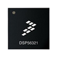
XC56309VL100A Freescale Semiconductor, XC56309VL100A Datasheet - Page 190

XC56309VL100A
Manufacturer Part Number
XC56309VL100A
Description
IC DSP 24BIT 100MHZ 196-MAPBGA
Manufacturer
Freescale Semiconductor
Series
DSP563xxr
Type
Fixed Pointr
Specifications of XC56309VL100A
Interface
Host Interface, SSI, SCI
Clock Rate
100MHz
Non-volatile Memory
ROM (576 B)
On-chip Ram
24kB
Voltage - I/o
3.30V
Voltage - Core
3.30V
Operating Temperature
-40°C ~ 100°C
Mounting Type
Surface Mount
Package / Case
196-MAPBGA
Device Core Size
24b
Format
Fixed Point
Clock Freq (max)
100MHz
Mips
100
Device Input Clock Speed
100MHz
Ram Size
102KB
Operating Supply Voltage (typ)
3.3V
Operating Supply Voltage (min)
3V
Operating Supply Voltage (max)
3.6V
Operating Temp Range
-40C to 100C
Operating Temperature Classification
Industrial
Mounting
Surface Mount
Pin Count
196
Package Type
MA-BGA
Lead Free Status / RoHS Status
Lead free / RoHS Compliant
Available stocks
Company
Part Number
Manufacturer
Quantity
Price
Company:
Part Number:
XC56309VL100A
Manufacturer:
Freescale Semiconductor
Quantity:
10 000
Company:
Part Number:
XC56309VL100AR2
Manufacturer:
Freescale Semiconductor
Quantity:
10 000
- Current page: 190 of 284
- Download datasheet (4Mb)
Serial Communication Interface (SCI)
addresses. If SCKP is set and SSHTD is set, SCI Synchronous mode is equivalent to the SSI
operation in 8-bit data on-demand mode.
Note:
8.7 GPIO Signals and Registers
Three registers control the GPIO functionality of the SCI pins: Port E control register (PCRE),
Port E direction register (PRRE) and Port E data register (PDRE).
8.7.1 Port E Control Register (PCRE)
The read/write PCRE controls the functionality of SCI GPIO signals. Each of the PCRE[2–0] bits
controls the functionality of the corresponding port signal. When a PCRE[i] bit is set, the
corresponding port signal is configured as an SCI signal. When a PC[i] bit is cleared, the
corresponding port signal is configured as a GPIO signal. A hardware
RESET instruction clears all PCRE bits.
8.7.2 Port E Direction Register (PRRE)
The read/write PRRE controls the direction of SCI GPIO signals. When port signal[i] is
configured as GPIO, PRRE[i] controls the port signal direction. When PRRE[i] is set, the GPIO
port signal[i] is configured as output. When PRRE[i] is cleared, the GPIO port signal[i] is
8-22
Note:
23
11
For bits 2–0, a 0 selects PEn as the signal and a 1 selects the specified SCI signal.
= Reserved. Read as zero. Write to zero for future compatibility.
When data is written to a peripheral device, there is a two-cycle pipeline delay until
any status bits affected by this operation are updated. If you read any of those status
bits within the next two cycles, the bit does not reflect its current status. For details see
the DSP56300 Family Manual.
22
10
21
Figure 8-8. Port E Control Register (PCRE X:$FFFF9F)
9
20
8
DSP56309 User’s Manual, Rev. 1
19
7
18
6
17
5
16
4
15
3
RESET
SCLK
PE2/
14
2
signal or a software
Freescale Semiconductor
PE1/
TXD
13
1
PE0/
RXD
12
0
Related parts for XC56309VL100A
Image
Part Number
Description
Manufacturer
Datasheet
Request
R
Part Number:
Description:
Manufacturer:
Freescale Semiconductor, Inc
Datasheet:
Part Number:
Description:
Manufacturer:
Freescale Semiconductor, Inc
Datasheet:
Part Number:
Description:
Manufacturer:
Freescale Semiconductor, Inc
Datasheet:
Part Number:
Description:
Manufacturer:
Freescale Semiconductor, Inc
Datasheet:
Part Number:
Description:
Manufacturer:
Freescale Semiconductor, Inc
Datasheet:
Part Number:
Description:
Manufacturer:
Freescale Semiconductor, Inc
Datasheet:
Part Number:
Description:
Manufacturer:
Freescale Semiconductor, Inc
Datasheet:
Part Number:
Description:
Manufacturer:
Freescale Semiconductor, Inc
Datasheet:
Part Number:
Description:
Manufacturer:
Freescale Semiconductor, Inc
Datasheet:
Part Number:
Description:
Manufacturer:
Freescale Semiconductor, Inc
Datasheet:
Part Number:
Description:
Manufacturer:
Freescale Semiconductor, Inc
Datasheet:
Part Number:
Description:
Manufacturer:
Freescale Semiconductor, Inc
Datasheet:
Part Number:
Description:
Manufacturer:
Freescale Semiconductor, Inc
Datasheet:
Part Number:
Description:
Manufacturer:
Freescale Semiconductor, Inc
Datasheet:
Part Number:
Description:
Manufacturer:
Freescale Semiconductor, Inc
Datasheet:


