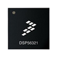
XC56309VL100A Freescale Semiconductor, XC56309VL100A Datasheet - Page 133

XC56309VL100A
Manufacturer Part Number
XC56309VL100A
Description
IC DSP 24BIT 100MHZ 196-MAPBGA
Manufacturer
Freescale Semiconductor
Series
DSP563xxr
Type
Fixed Pointr
Specifications of XC56309VL100A
Interface
Host Interface, SSI, SCI
Clock Rate
100MHz
Non-volatile Memory
ROM (576 B)
On-chip Ram
24kB
Voltage - I/o
3.30V
Voltage - Core
3.30V
Operating Temperature
-40°C ~ 100°C
Mounting Type
Surface Mount
Package / Case
196-MAPBGA
Device Core Size
24b
Format
Fixed Point
Clock Freq (max)
100MHz
Mips
100
Device Input Clock Speed
100MHz
Ram Size
102KB
Operating Supply Voltage (typ)
3.3V
Operating Supply Voltage (min)
3V
Operating Supply Voltage (max)
3.6V
Operating Temp Range
-40C to 100C
Operating Temperature Classification
Industrial
Mounting
Surface Mount
Pin Count
196
Package Type
MA-BGA
Lead Free Status / RoHS Status
Lead free / RoHS Compliant
Available stocks
Company
Part Number
Manufacturer
Quantity
Price
Company:
Part Number:
XC56309VL100A
Manufacturer:
Freescale Semiconductor
Quantity:
10 000
Company:
Part Number:
XC56309VL100AR2
Manufacturer:
Freescale Semiconductor
Quantity:
10 000
- Current page: 133 of 284
- Download datasheet (4Mb)
Enhanced Synchronous Serial Interface
(ESSI)
The ESSI provides a full-duplex serial port for serial communication with a variety of serial
devices, including one or more industry-standard codecs, other DSPs, microprocessors, and
peripherals. The ESSI consists of independent transmitter and receiver sections and a common
ESSI clock generator. There are two independent and identical ESSIs in the DSP56309: ESSI0
and ESSI1. For simplicity, a single generic ESSI is described here. The ESSI block diagram is
shown in Figure 7-1. This interface is synchronous because all serial transfers are synchronized
to one clock.
This synchronous interface should not be confused with the asynchronous channels mode of the
ESSI, in which separate clocks are used for the receiver and transmitter. In that mode, the ESSI is
still a synchronous device because all transfers are synchronized to these clocks. Pin notations for
the generic ESSI refer to the analogous pin of ESSI0 (
Freescale Semiconductor
Interrupts
Clock/Frame Sync Generators and Control Logic
Figure 7-1. ESSI Block Diagram
DSP56309 User’s Manual, Rev. 1
RSMB
SSISR
RSMA
TSMA
TSMB
CRB
CRA
TSR
GDB
DDB
RCLK
TCLK
PCx
) and ESSI1 (
RX SHIFT REG
TX2 SHIFT
TX0 SHIFT REG
TX1 SHIFT REG
TX0
TX2
TX1
RX
PDx
STD
SC0
SC1
SC2
SCK
SRD
).
7
7-1
Related parts for XC56309VL100A
Image
Part Number
Description
Manufacturer
Datasheet
Request
R
Part Number:
Description:
Manufacturer:
Freescale Semiconductor, Inc
Datasheet:
Part Number:
Description:
Manufacturer:
Freescale Semiconductor, Inc
Datasheet:
Part Number:
Description:
Manufacturer:
Freescale Semiconductor, Inc
Datasheet:
Part Number:
Description:
Manufacturer:
Freescale Semiconductor, Inc
Datasheet:
Part Number:
Description:
Manufacturer:
Freescale Semiconductor, Inc
Datasheet:
Part Number:
Description:
Manufacturer:
Freescale Semiconductor, Inc
Datasheet:
Part Number:
Description:
Manufacturer:
Freescale Semiconductor, Inc
Datasheet:
Part Number:
Description:
Manufacturer:
Freescale Semiconductor, Inc
Datasheet:
Part Number:
Description:
Manufacturer:
Freescale Semiconductor, Inc
Datasheet:
Part Number:
Description:
Manufacturer:
Freescale Semiconductor, Inc
Datasheet:
Part Number:
Description:
Manufacturer:
Freescale Semiconductor, Inc
Datasheet:
Part Number:
Description:
Manufacturer:
Freescale Semiconductor, Inc
Datasheet:
Part Number:
Description:
Manufacturer:
Freescale Semiconductor, Inc
Datasheet:
Part Number:
Description:
Manufacturer:
Freescale Semiconductor, Inc
Datasheet:
Part Number:
Description:
Manufacturer:
Freescale Semiconductor, Inc
Datasheet:


