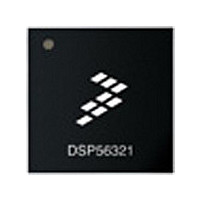
XC56309VL100A Freescale Semiconductor, XC56309VL100A Datasheet - Page 84

XC56309VL100A
Manufacturer Part Number
XC56309VL100A
Description
IC DSP 24BIT 100MHZ 196-MAPBGA
Manufacturer
Freescale Semiconductor
Series
DSP563xxr
Type
Fixed Pointr
Specifications of XC56309VL100A
Interface
Host Interface, SSI, SCI
Clock Rate
100MHz
Non-volatile Memory
ROM (576 B)
On-chip Ram
24kB
Voltage - I/o
3.30V
Voltage - Core
3.30V
Operating Temperature
-40°C ~ 100°C
Mounting Type
Surface Mount
Package / Case
196-MAPBGA
Device Core Size
24b
Format
Fixed Point
Clock Freq (max)
100MHz
Mips
100
Device Input Clock Speed
100MHz
Ram Size
102KB
Operating Supply Voltage (typ)
3.3V
Operating Supply Voltage (min)
3V
Operating Supply Voltage (max)
3.6V
Operating Temp Range
-40C to 100C
Operating Temperature Classification
Industrial
Mounting
Surface Mount
Pin Count
196
Package Type
MA-BGA
Lead Free Status / RoHS Status
Lead free / RoHS Compliant
Available stocks
Company
Part Number
Manufacturer
Quantity
Price
Company:
Part Number:
XC56309VL100A
Manufacturer:
Freescale Semiconductor
Quantity:
10 000
Company:
Part Number:
XC56309VL100AR2
Manufacturer:
Freescale Semiconductor
Quantity:
10 000
- Current page: 84 of 284
- Download datasheet (4Mb)
Core Configuration
4.6.3 Address Attribute Registers (AAR[0–3])
The Address Attribute Registers (AAR[0–3]) are read/write registers that control the activity of
the
the BAC bits in the associated AAR matches the exact number of external address bits defined by
the BNC bits, and the external address space (X data, Y data, or program) is enabled by the AAR.
Figure 4-8 shows an AAR register; Table 4-10 lists the bit definitions.
Note:
4-26
Number
23–12
11–8
Bit
AA0
BAC11
BNC3
/
RAS0
11
23
Figure 4-8. Address Attribute Registers (AAR[0–3]) (X:$FFFFF9–$FFFFF6)
Bit Name
The DSP56309 does not support address multiplexing.
BAC
BNC
BAC10
BNC2
–
Reserved Bit. Write to zero for future compatibility.
10
22
Table 4-10. Address Attribute Registers (AAR[0–3]) Bit Definitions
AA3
BNC1
BAC9
/
RAS3
21
9
Reset
Value
0
0
BNC0
BAC8
20
8
pins. The associated
Bus Address to Compare
Read/write control bits that define the upper 12 bits of the 24-bit address with which to
compare the external address to determine whether to assert the corresponding AA/RAS
signal. This is also true of 16-bit compatibility mode. The BNC[3–0] bits define the number of
address bits to compare.
Bus Number of Address Bits to Compare
Specify the number of bits (from the BAC bits) that are compared to the external address.
The BAC bits are always compared with the Most Significant Portion of the external address
(for example, if BNC[3–0] = 0011, then the BAC[11–9] bits are compared to the 3 MSBs of
the external address). If no bits are specified (that is, BNC[3–0] = 0000), the AA signal is
activated for the entire 16 M-word space identified by the space enable bits (BPEN, BXEN,
BYEN), but only when the address is external to the internal memory map. The
combinations BNC[3–0] = 1111, 1110, 1101 are reserved.
BPAC
BAC7 BAC6
19
7
18
6
DSP56309 User’s Manual, Rev. 1
BYEN
BAC5
17
5
BXEN
BAC4
16
4
AAn
BPEN
BAC3 BAC2
/
RASn
3
15
BAAP
2
14
pin is asserted if the address defined by
Description
BAT1
BAC1
13
1
BAT0
BAC0
0
12
External Access Type
AA pin polarity
Program space Enable
X data space Enable
Y data space Enable
Reserved
Packing Enable
Number of Address bit to
compare
Address to Compare
Freescale Semiconductor
Related parts for XC56309VL100A
Image
Part Number
Description
Manufacturer
Datasheet
Request
R
Part Number:
Description:
Manufacturer:
Freescale Semiconductor, Inc
Datasheet:
Part Number:
Description:
Manufacturer:
Freescale Semiconductor, Inc
Datasheet:
Part Number:
Description:
Manufacturer:
Freescale Semiconductor, Inc
Datasheet:
Part Number:
Description:
Manufacturer:
Freescale Semiconductor, Inc
Datasheet:
Part Number:
Description:
Manufacturer:
Freescale Semiconductor, Inc
Datasheet:
Part Number:
Description:
Manufacturer:
Freescale Semiconductor, Inc
Datasheet:
Part Number:
Description:
Manufacturer:
Freescale Semiconductor, Inc
Datasheet:
Part Number:
Description:
Manufacturer:
Freescale Semiconductor, Inc
Datasheet:
Part Number:
Description:
Manufacturer:
Freescale Semiconductor, Inc
Datasheet:
Part Number:
Description:
Manufacturer:
Freescale Semiconductor, Inc
Datasheet:
Part Number:
Description:
Manufacturer:
Freescale Semiconductor, Inc
Datasheet:
Part Number:
Description:
Manufacturer:
Freescale Semiconductor, Inc
Datasheet:
Part Number:
Description:
Manufacturer:
Freescale Semiconductor, Inc
Datasheet:
Part Number:
Description:
Manufacturer:
Freescale Semiconductor, Inc
Datasheet:
Part Number:
Description:
Manufacturer:
Freescale Semiconductor, Inc
Datasheet:


