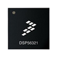
XC56309VL100A Freescale Semiconductor, XC56309VL100A Datasheet - Page 79

XC56309VL100A
Manufacturer Part Number
XC56309VL100A
Description
IC DSP 24BIT 100MHZ 196-MAPBGA
Manufacturer
Freescale Semiconductor
Series
DSP563xxr
Type
Fixed Pointr
Specifications of XC56309VL100A
Interface
Host Interface, SSI, SCI
Clock Rate
100MHz
Non-volatile Memory
ROM (576 B)
On-chip Ram
24kB
Voltage - I/o
3.30V
Voltage - Core
3.30V
Operating Temperature
-40°C ~ 100°C
Mounting Type
Surface Mount
Package / Case
196-MAPBGA
Device Core Size
24b
Format
Fixed Point
Clock Freq (max)
100MHz
Mips
100
Device Input Clock Speed
100MHz
Ram Size
102KB
Operating Supply Voltage (typ)
3.3V
Operating Supply Voltage (min)
3V
Operating Supply Voltage (max)
3.6V
Operating Temp Range
-40C to 100C
Operating Temperature Classification
Industrial
Mounting
Surface Mount
Pin Count
196
Package Type
MA-BGA
Lead Free Status / RoHS Status
Lead free / RoHS Compliant
Available stocks
Company
Part Number
Manufacturer
Quantity
Price
Company:
Part Number:
XC56309VL100A
Manufacturer:
Freescale Semiconductor
Quantity:
10 000
Company:
Part Number:
XC56309VL100AR2
Manufacturer:
Freescale Semiconductor
Quantity:
10 000
- Current page: 79 of 284
- Download datasheet (4Mb)
4.6 Bus Interface Unit (BIU) Registers
The three Bus Interface Unit (BIU) registers configure the external memory expansion port (Port
A). They include the following:
To use Port A correctly, configure these registers as part of the bootstrap process. The following
subsections describe these registers.
4.6.1 Bus Control Register (BCR)
The Bus Control Register (BCR), depicted in Figure 4-6, is a read/write register that controls the
external bus activity and Bus Interface Unit (BIU) operation. All BCR bits except bit 21, BBS,
are read/write bits. The BCR bits are defined in Table 4-8.
Freescale Semiconductor
BA2W1
Bit Number
BRH
23
11
14–12
11–0
15
Bus Control Register (BCR)
DRAM Control Register (DCR)
Address Attribute Registers (AAR[3–0])
Reserved bit. Read as zero; write to zero for future compatibility
BA2W0
22
10
Bit Name
MF[11–0]
Table 4-7. PLL Control Register (PCTL) Bit Definitions (Continued)
DF[2–0]
XTLR
BA1W4
BBS
21
9
Reset Value
BDFW4
BA1W3
20
8
Figure 4-6. Bus Control Register (BCR)
0
0
0
BDFW3
BA1W2
19
DSP56309 User’s Manual, Rev. 1
7
Crystal Range
Controls the internal crystal oscillator transconductance. The XTLR bit is
cleared (0) during hardware reset.
Division Factor
Define the DF of the low-power divider. These bits specify the DF as a power
of two in the range from 2
PLL Multiplication Factor
Define the multiplication factor that is applied to the PLL input frequency. The
MF bits are cleared during hardware reset and thus correspond to an MF of
one.
BDFW2
BA1W1
18
6
BDFW1
BA1W0
17
5
0
to 2
BDFW0
BA0W4
16
7
4
.
Description
BA3W2
BA0W3
15
3
Bus Interface Unit (BIU) Registers
BA3W1
BA0W2
14
2
BA3W0
BA0W1
13
1
BA2W2
BA0W0
12
0
4-21
Related parts for XC56309VL100A
Image
Part Number
Description
Manufacturer
Datasheet
Request
R
Part Number:
Description:
Manufacturer:
Freescale Semiconductor, Inc
Datasheet:
Part Number:
Description:
Manufacturer:
Freescale Semiconductor, Inc
Datasheet:
Part Number:
Description:
Manufacturer:
Freescale Semiconductor, Inc
Datasheet:
Part Number:
Description:
Manufacturer:
Freescale Semiconductor, Inc
Datasheet:
Part Number:
Description:
Manufacturer:
Freescale Semiconductor, Inc
Datasheet:
Part Number:
Description:
Manufacturer:
Freescale Semiconductor, Inc
Datasheet:
Part Number:
Description:
Manufacturer:
Freescale Semiconductor, Inc
Datasheet:
Part Number:
Description:
Manufacturer:
Freescale Semiconductor, Inc
Datasheet:
Part Number:
Description:
Manufacturer:
Freescale Semiconductor, Inc
Datasheet:
Part Number:
Description:
Manufacturer:
Freescale Semiconductor, Inc
Datasheet:
Part Number:
Description:
Manufacturer:
Freescale Semiconductor, Inc
Datasheet:
Part Number:
Description:
Manufacturer:
Freescale Semiconductor, Inc
Datasheet:
Part Number:
Description:
Manufacturer:
Freescale Semiconductor, Inc
Datasheet:
Part Number:
Description:
Manufacturer:
Freescale Semiconductor, Inc
Datasheet:
Part Number:
Description:
Manufacturer:
Freescale Semiconductor, Inc
Datasheet:


