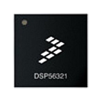
XC56309VL100A Freescale Semiconductor, XC56309VL100A Datasheet - Page 91

XC56309VL100A
Manufacturer Part Number
XC56309VL100A
Description
IC DSP 24BIT 100MHZ 196-MAPBGA
Manufacturer
Freescale Semiconductor
Series
DSP563xxr
Type
Fixed Pointr
Specifications of XC56309VL100A
Interface
Host Interface, SSI, SCI
Clock Rate
100MHz
Non-volatile Memory
ROM (576 B)
On-chip Ram
24kB
Voltage - I/o
3.30V
Voltage - Core
3.30V
Operating Temperature
-40°C ~ 100°C
Mounting Type
Surface Mount
Package / Case
196-MAPBGA
Device Core Size
24b
Format
Fixed Point
Clock Freq (max)
100MHz
Mips
100
Device Input Clock Speed
100MHz
Ram Size
102KB
Operating Supply Voltage (typ)
3.3V
Operating Supply Voltage (min)
3V
Operating Supply Voltage (max)
3.6V
Operating Temp Range
-40C to 100C
Operating Temperature Classification
Industrial
Mounting
Surface Mount
Pin Count
196
Package Type
MA-BGA
Lead Free Status / RoHS Status
Lead free / RoHS Compliant
Available stocks
Company
Part Number
Manufacturer
Quantity
Price
Company:
Part Number:
XC56309VL100A
Manufacturer:
Freescale Semiconductor
Quantity:
10 000
Company:
Part Number:
XC56309VL100AR2
Manufacturer:
Freescale Semiconductor
Quantity:
10 000
- Current page: 91 of 284
- Download datasheet (4Mb)
4.8 Device Identification Register (IDR)
The IDR is a read-only factory-programmed register that identifies DSP56300 family members.
It specifies the derivative number and revision number of the device. This information is used in
testing or by software. Figure 4-10 shows the contents of the IDR. Revision numbers are
assigned as follows: $0 is revision 0, $1 is revision A, and so on.
.
Freescale Semiconductor
Number
9–4
3–2
1–0
Bit
Bit Name
DDS[1–0]
DAM
DSS
Table 4-11. DMA Control Register (DCR) Bit Definitions (Continued)
23
Figure 4-10. Identification Register Configuration (Revision E)
Reserved
Reset
Value
$00
0
0
0
DMA Address Mode
Defines the address generation mode for the DMA transfer. These bits are encoded in two
different ways according to the D3D bit.
DMA Destination Space
Specify the memory space referenced as a destination by the DMA.
Note:
DMA Source Space
Specify the memory space referenced as a source by the DMA.
Note:
16
15
DDS1
DSS1
In Cache mode, a DMA to Program memory space has some limitations (as
described in Chapter 3, Memory Configuration .
In Cache mode, a DMA to Program memory space has some limitations (as
described in Chapter 3, Memory Configuration .
Revision Number
0
0
1
1
0
0
1
1
DSP56309 User’s Manual, Rev. 1
$5
12
DDS0
DSS0
0
1
0
1
0
1
0
1
11
Description
Derivative Number
X Memory Space
Y Memory Space
P Memory Space
Reserved
X Memory Space
Y Memory Space
P Memory Space
Reserved
DMA Destination Memory Space
$303
DMA Source Memory Space
Device Identification Register (IDR)
0
4-33
Related parts for XC56309VL100A
Image
Part Number
Description
Manufacturer
Datasheet
Request
R
Part Number:
Description:
Manufacturer:
Freescale Semiconductor, Inc
Datasheet:
Part Number:
Description:
Manufacturer:
Freescale Semiconductor, Inc
Datasheet:
Part Number:
Description:
Manufacturer:
Freescale Semiconductor, Inc
Datasheet:
Part Number:
Description:
Manufacturer:
Freescale Semiconductor, Inc
Datasheet:
Part Number:
Description:
Manufacturer:
Freescale Semiconductor, Inc
Datasheet:
Part Number:
Description:
Manufacturer:
Freescale Semiconductor, Inc
Datasheet:
Part Number:
Description:
Manufacturer:
Freescale Semiconductor, Inc
Datasheet:
Part Number:
Description:
Manufacturer:
Freescale Semiconductor, Inc
Datasheet:
Part Number:
Description:
Manufacturer:
Freescale Semiconductor, Inc
Datasheet:
Part Number:
Description:
Manufacturer:
Freescale Semiconductor, Inc
Datasheet:
Part Number:
Description:
Manufacturer:
Freescale Semiconductor, Inc
Datasheet:
Part Number:
Description:
Manufacturer:
Freescale Semiconductor, Inc
Datasheet:
Part Number:
Description:
Manufacturer:
Freescale Semiconductor, Inc
Datasheet:
Part Number:
Description:
Manufacturer:
Freescale Semiconductor, Inc
Datasheet:
Part Number:
Description:
Manufacturer:
Freescale Semiconductor, Inc
Datasheet:


