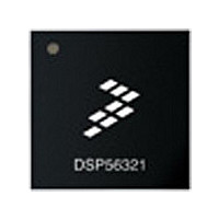
XC56309VL100A Freescale Semiconductor, XC56309VL100A Datasheet - Page 208

XC56309VL100A
Manufacturer Part Number
XC56309VL100A
Description
IC DSP 24BIT 100MHZ 196-MAPBGA
Manufacturer
Freescale Semiconductor
Series
DSP563xxr
Type
Fixed Pointr
Specifications of XC56309VL100A
Interface
Host Interface, SSI, SCI
Clock Rate
100MHz
Non-volatile Memory
ROM (576 B)
On-chip Ram
24kB
Voltage - I/o
3.30V
Voltage - Core
3.30V
Operating Temperature
-40°C ~ 100°C
Mounting Type
Surface Mount
Package / Case
196-MAPBGA
Device Core Size
24b
Format
Fixed Point
Clock Freq (max)
100MHz
Mips
100
Device Input Clock Speed
100MHz
Ram Size
102KB
Operating Supply Voltage (typ)
3.3V
Operating Supply Voltage (min)
3V
Operating Supply Voltage (max)
3.6V
Operating Temp Range
-40C to 100C
Operating Temperature Classification
Industrial
Mounting
Surface Mount
Pin Count
196
Package Type
MA-BGA
Lead Free Status / RoHS Status
Lead free / RoHS Compliant
Available stocks
Company
Part Number
Manufacturer
Quantity
Price
Company:
Part Number:
XC56309VL100A
Manufacturer:
Freescale Semiconductor
Quantity:
10 000
Company:
Part Number:
XC56309VL100AR2
Manufacturer:
Freescale Semiconductor
Quantity:
10 000
- Current page: 208 of 284
- Download datasheet (4Mb)
Triple Timer Module
9.3.3 Pulse Width Modulation
In Mode 7, the timer generates periodic pulses of a preset width. When the counter equals the
value in the TCPR, the
counter are placed into the TCR. If the TCSR[TCIE] bit is set, a compare interrupt is generated.
The counter continues to increment on each timer clock.
If counter overflow occurs, the
interrupt is generated if the TCSR[TOIE] bit is set. If the TCSR[TRM] bit is set, the counter is
loaded with the TLR value on the next timer clock and the count resumes. If the TCSR[TRM] bit
is cleared, the counter continues to increment on each timer clock. This process repeats until the
timer is disabled.
When the TCSR[TE] bit is set and the counter starts, the
each subsequent toggle of the
the INV bit is set, the
TIO
The value of the TLR determines the output period ($FFFFFF − TLR + 1). The timer counter
increments the initial TLR value and toggles the
$FFFFFF. The duty cycle of the
value in the TLR increments to a value equal to the value in the TCPR, the
The duty cycle is equal to ($FFFFFF – TCPR) divided by ($FFFFFF − TLR + 1). For a 50 percent
duty cycle, the value of TCPR is equal to ($FFFFFF + TLR + 1)/2.
Note:
9-16
TC3
0
signal generates the following signal: 0101.
TC2
The value in TCPR must be greater than the value in TLR.
Bit Settings
1
TC1
1
TIO
TIO
TC0
signal generates the following signal: 1010. If the INV bit is cleared, the
1
output signal is toggled and TCSR[TCF] is set. The contents of the
TIO
TIO
TIO
Mode
signal, the polarity of the
7
output signal is toggled, TCSR[TOF] is set, and an overflow
DSP56309 User’s Manual, Rev. 1
signal is determined by the value in the TCPR. When the
Pulse width modulation
Name
TIO
signal when the counter value exceeds
Mode Characteristics
TIO
TIO
signal assumes the value of INV. On
signal is reversed. For example, if
Function
PWM
TIO
Freescale Semiconductor
Output
TIO
signal is toggled.
Internal
Clock
Related parts for XC56309VL100A
Image
Part Number
Description
Manufacturer
Datasheet
Request
R
Part Number:
Description:
Manufacturer:
Freescale Semiconductor, Inc
Datasheet:
Part Number:
Description:
Manufacturer:
Freescale Semiconductor, Inc
Datasheet:
Part Number:
Description:
Manufacturer:
Freescale Semiconductor, Inc
Datasheet:
Part Number:
Description:
Manufacturer:
Freescale Semiconductor, Inc
Datasheet:
Part Number:
Description:
Manufacturer:
Freescale Semiconductor, Inc
Datasheet:
Part Number:
Description:
Manufacturer:
Freescale Semiconductor, Inc
Datasheet:
Part Number:
Description:
Manufacturer:
Freescale Semiconductor, Inc
Datasheet:
Part Number:
Description:
Manufacturer:
Freescale Semiconductor, Inc
Datasheet:
Part Number:
Description:
Manufacturer:
Freescale Semiconductor, Inc
Datasheet:
Part Number:
Description:
Manufacturer:
Freescale Semiconductor, Inc
Datasheet:
Part Number:
Description:
Manufacturer:
Freescale Semiconductor, Inc
Datasheet:
Part Number:
Description:
Manufacturer:
Freescale Semiconductor, Inc
Datasheet:
Part Number:
Description:
Manufacturer:
Freescale Semiconductor, Inc
Datasheet:
Part Number:
Description:
Manufacturer:
Freescale Semiconductor, Inc
Datasheet:
Part Number:
Description:
Manufacturer:
Freescale Semiconductor, Inc
Datasheet:


