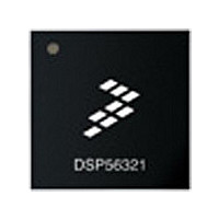
XC56309VL100A Freescale Semiconductor, XC56309VL100A Datasheet - Page 169

XC56309VL100A
Manufacturer Part Number
XC56309VL100A
Description
IC DSP 24BIT 100MHZ 196-MAPBGA
Manufacturer
Freescale Semiconductor
Series
DSP563xxr
Type
Fixed Pointr
Specifications of XC56309VL100A
Interface
Host Interface, SSI, SCI
Clock Rate
100MHz
Non-volatile Memory
ROM (576 B)
On-chip Ram
24kB
Voltage - I/o
3.30V
Voltage - Core
3.30V
Operating Temperature
-40°C ~ 100°C
Mounting Type
Surface Mount
Package / Case
196-MAPBGA
Device Core Size
24b
Format
Fixed Point
Clock Freq (max)
100MHz
Mips
100
Device Input Clock Speed
100MHz
Ram Size
102KB
Operating Supply Voltage (typ)
3.3V
Operating Supply Voltage (min)
3V
Operating Supply Voltage (max)
3.6V
Operating Temp Range
-40C to 100C
Operating Temperature Classification
Industrial
Mounting
Surface Mount
Pin Count
196
Package Type
MA-BGA
Lead Free Status / RoHS Status
Lead free / RoHS Compliant
Available stocks
Company
Part Number
Manufacturer
Quantity
Price
Company:
Part Number:
XC56309VL100A
Manufacturer:
Freescale Semiconductor
Quantity:
10 000
Company:
Part Number:
XC56309VL100AR2
Manufacturer:
Freescale Semiconductor
Quantity:
10 000
- Current page: 169 of 284
- Download datasheet (4Mb)
Serial Communication Interface (SCI)
The SCI provides a full-duplex port for serial communication with other DSPs, microprocessors,
or peripherals such as modems. The SCI interfaces without additional logic to peripherals that
use TTL-level signals. With a small amount of additional logic, the SCI can connect to peripheral
interfaces that have non-TTL level signals, such as RS-232, RS-422, and so on. This interface
uses three dedicated signals: transmit data, receive data, and SCI serial clock. It supports
industry-standard asynchronous bit rates and protocols, as well as high-speed synchronous data
transmission. SCI asynchronous protocols include a multidrop mode for master/slave operation
with wake-up on idle line and wake-up on address bit capability. This mode allows the
DSP56309 to share a single serial line efficiently with other peripherals.
The SCI consists of separate transmit and receive sections that can operate asynchronously with
respect to each other. A programmable baud rate generator supplies the transmit and receive
clocks. An enable vector and an interrupt vector are included so that the baud-rate generator can
function as a general-purpose timer when the SCI is not using it, or when the interrupt timing is
the same as that used by the SCI.
8.1 Operating Modes
The operating modes for the DSP56309 SCI are as follows:
These modes are selected by the SCR WD[2–0] bits. Synchronous data mode is essentially a
high-speed shift register for I/O expansion and stream-mode channel interfaces. A gated transmit
and receive clock compatible with the Intel 8051 serial interface mode 0 synchronizes data.
Asynchronous modes are compatible with most UART-type serial devices. Standard RS-232
communication links are supported by these modes. Multidrop Asynchronous mode is
Freescale Semiconductor
8-bit synchronous (shift register mode)
10-bit asynchronous (1 start, 8 data, 1 stop)
11-bit asynchronous (1 start, 8 data, 1 even parity, 1 stop)
11-bit asynchronous (1 start, 8 data, 1 odd parity, 1 stop)
11-bit multidrop asynchronous (1 start, 8 data, 1 data type, 1 stop)
This mode is used for master/slave operation with wake-up on idle line and wake-up on
address bit capability. It allows the DSP56309 to share a single serial line efficiently with
other peripherals.
DSP56309 User’s Manual, Rev. 1
8
8-1
Related parts for XC56309VL100A
Image
Part Number
Description
Manufacturer
Datasheet
Request
R
Part Number:
Description:
Manufacturer:
Freescale Semiconductor, Inc
Datasheet:
Part Number:
Description:
Manufacturer:
Freescale Semiconductor, Inc
Datasheet:
Part Number:
Description:
Manufacturer:
Freescale Semiconductor, Inc
Datasheet:
Part Number:
Description:
Manufacturer:
Freescale Semiconductor, Inc
Datasheet:
Part Number:
Description:
Manufacturer:
Freescale Semiconductor, Inc
Datasheet:
Part Number:
Description:
Manufacturer:
Freescale Semiconductor, Inc
Datasheet:
Part Number:
Description:
Manufacturer:
Freescale Semiconductor, Inc
Datasheet:
Part Number:
Description:
Manufacturer:
Freescale Semiconductor, Inc
Datasheet:
Part Number:
Description:
Manufacturer:
Freescale Semiconductor, Inc
Datasheet:
Part Number:
Description:
Manufacturer:
Freescale Semiconductor, Inc
Datasheet:
Part Number:
Description:
Manufacturer:
Freescale Semiconductor, Inc
Datasheet:
Part Number:
Description:
Manufacturer:
Freescale Semiconductor, Inc
Datasheet:
Part Number:
Description:
Manufacturer:
Freescale Semiconductor, Inc
Datasheet:
Part Number:
Description:
Manufacturer:
Freescale Semiconductor, Inc
Datasheet:
Part Number:
Description:
Manufacturer:
Freescale Semiconductor, Inc
Datasheet:


